X-Ray Inspection – Lead-Free Solder Drives X-Ray Inspection
X-ray and advanced automated techniques combine to create a capable tool for lead-free solder inspection needs.
Within two years, solder used in electronics manufactured or sold in Europe must meet the European Restrictions on Hazardous Substances (RoHS) and Waste Electrical and Electronic Equipment (WEEE) lead-free standards. Similar standards must be met for Japan even sooner. As a result, many manufacturers are beginning the shift to lead-free solder alloys and glues which, in turn, has raised concerns about whether their current inspection and quality-control procedures will still be valid.
This is especially true for X-ray inspection. With lead solder, joints are easily interpreted by the operator or the system imaging software because lead provides excellent image contrasts due to relatively high X-ray absorption compared to that of PCB and component materials. Will lead-free solders offer the same contrast? What new features or procedures will be needed for better, more accurate inspection techniques?
X-Ray Imaging Basics
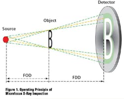
To understand the suitability of X-ray systems for the inspection of lead-free interconnections, let's begin with a review of the physics of X-ray imaging. Whether microfocus or nanofocus, X-rays penetrate a specimen using a cone-shaped beam that generates a magnified X-ray shadow image on the detector. The achievable resolution or image sharpness principally is influenced by the focal-spot size of the X-ray tube, which varies from a few microns for a microfocus tube to less than 1 micron for the latest nanofocus tubes.
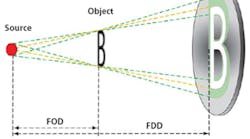
Image magnification, a key feature for analysis, is determined by the beam's geometry (Figure 1) and defined as:
Geometric Magnification = FDD/FOD
where: FOD = focus object distance, the focal distance from
the bottom of the tube to the test object
FDD = focus detector distance, the distance
from the tube to the image detector
At higher magnifications, image resolution is limited by the focal-spot size of the X-ray source. This limitation is caused by image blurring or the Penumbra effect resulting from a loss in image definition attributed to the finite size of the spot, as illustrated by the green shadow in Figure 1.
Another consideration is the image contrast. Contrast is affected by the differing X-ray absorptions of the various inspection targets on a PCB due to variations in thickness of the solder joints or in material, like solder on a copper land.
X-ray absorption is defined by this exponential law:
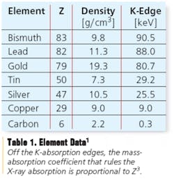
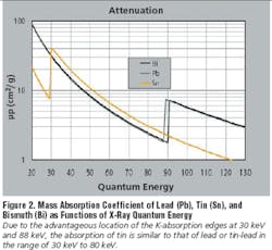
/ρ = the material's influence as defined by the mass absorption coefficient that also depends on the energy E of the radiation quanta ρ = the density of the material of thickness xThe mass absorption coefficient /ρ can be approximated using the cube of the material's atomic number Z3. See Table 1 for Z values of common lead-free materials.
Lead-Free Contrasts
Currently, most lead-free solders consist mainly of tin or Bismuth. For Bismuth (Z = 83), X-ray absorption is expected to be comparable to lead (Z = 82) solders (PbSn); tin solders (Z = 50) should have much lower absorption and significantly poorer contrast.
As experience in the field has demonstrated, all typical test criteria for solder-joint integrity and all expected signatures of the soldering process are clearly visible and valid for lead-free solder joints. Moreover, with adequate X-ray equipment, there are no restrictions concerning the automatic inspection and evaluation of lead-free BGA and CSP solder joints.
This has been proven within the scope of an investigation of void development in lead-free PBGA solder joints (Sn96Ag4 and Sn95.5Ag4Cu0.5).1 Due to the small grey-value differences between the lead and lead-free solder, even mixed lots could be evaluated by the auto-setup BGA evaluation software without changing thresholds or X-ray parameters.
Increasing Defect Coverage
Traditionally, semi-automatic X-ray inspection equipment has offered advanced automated software tools for the analysis of BGA solder balls. The leading X-ray suppliers have improved these tools and increased BGA defect coverage to include void analysis, diameter measurements, roundness checks, and automated wetting analysis as well as basic ball presence/absence and bridging detection.
Similarly, these suppliers offer AXI tools for IC packaging applications. In the IC world, automated void detection for conductive and nonconductive die-attach, solder-bump inspection, wire-bond integrity, and wire-sweep measurement are common capabilities.
For BGA, CSP, and flip-chip applications, automated inspection using oblique views has increased defect coverage significantly in recent years. AXI based on oblique viewing provides two powerful advantages:
• Angled views and rotation of the sample allow the programmer to maximize signal-to-noise ratios in challenging inspection applications, such as double-sided reflow where signals from the other side of the PCB limit, blur, or deform the signal of the primary inspection target.
• Oblique viewing enables automated wetting inspection, a capability that is just now being implemented.
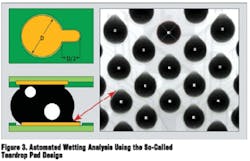
By changing the pad design to enhance the signal-to-noise ratio for wetting analysis, it now is feasible to automate this task. The pad design shown in Figure 3 does not impact the solder-joint integrity of the BGA ball. But by forcing the solder to flow onto the pad extension, a very strong signal is created that indicates successful wetting of the ball to the pad. Because the signal-to-noise ratio is high, automated inspection in an oblique view becomes possible.
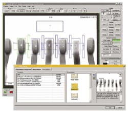
Customers and potential users of semi-automatic X-ray equipment continue to approach vendors with the desire to extend their automated defect coverage beyond the standard BGA coverage. Typical applications include the inspection of gull-wing devices such as QFP (Figure 4), PTH and connector pin applications, 0201 components, and many other customer-specific AXI needs.
Figure 4. Heel Fillet Inspection for QFPs The automated defect coverage in this application includes bent and lifted pin; presence and sufficiency of toe, side, and heel fillets; and voiding in the solder joint.
Adding these AXI measuring techniques increases the automated defect coverage without having to buy a fully automated machine. This is very beneficial for existing users.
The extra costs include the acquisition of the appropriate software module, programming time, and a potential increase in inspection cycle time. The cost savings result from less rework and scrap and substitution of test coverage from a later step in the manufacturing and test process to an earlier step, typically after reflow in the SMT process.
For example, a medium-sized electronics manufacturer recently added QFP solder-joint inspection to the existing BGA defect coverage. Although operators manually inspected for placement defects, bridging, and lifted leads, a shift to automated X-ray coverage led to a higher number of defects caught. The manufacturer gained additional defect coverage by inspecting the heel fillets and checking for voiding in the solder joint.
Conclusion
Refuting widespread doubts, lead-free and, in particular, tin-based solder joints are easily addressed by X-ray inspection. Using auto-setup software, inspection routines require few, if any, corrections.
To what extent should customary test criteria be changed for lead-free solder joints? That will be learned in future applications. At this point in time, at least the appearance of the Sn-based solder joints is quite similar to that of the PbSn solder joints, and systematic deviations in thickness or shape were not found.
To gain more process knowledge and control when switching to lead-free, it is desirable to increase AXI defect coverage beyond standard BGA applications. The tools now are becoming available to take semi-automatic X-ray equipment to the next level.
References
1. Lide, D.R. [ed.], CRC Handbook of Chemistry and Physics, 82, Auflage, Boca Raton 2001.
2. Reichenberger, M., Kozic, D., Roth, H., Bleifrei geht's auch, F & M 4/2001, S. 76-79.
About the Authors
Boris Mathiszik is vice president of sales at phoenix|x-ray's East Coast Division. He holds a degree in economics from the European Business School, Frankfurt, Germany, and an M.B.A. from San Diego State University. Mr. Mathiszik has more than eight years of experience in automated optical inspection and electronics in marketing, sales, and support management roles. 727-287-1508, email: [email protected]
Dr. Holger Roth is the applications manager at phoenix|x-ray Systems + Services GmbH, Wunstorf. He directs an inspection service laboratory in the Stuttgart branch of the company. e-mail: [email protected]
phoenix|x-ray Systems + Services, 100 First Avenue South, Suite 208,
St. Petersburg, FL 33701
