The Selection and Economics Of Wireless Test Fixtures
Wireless fixtures for in-circuit testing (ICT) have been available for more than 15 years and have no equal in testing high node-count complex circuit boards. However, there are other hidden advantages that apply to almost any board being tested, including decreased debug time, greater signal fidelity, increased capabilities to test low-voltage and multilogic modules, and reduced signal crosstalk. Obtaining these performance advantages for low node-count fixtures may require a longer payback period to cover the additional cost of the PCB used in the fixture.
As electronic devices get progressively denser and more complex, fixturing requirements become more demanding. Test pads are smaller and more closely spaced, voltages drop, and the potential for crosstalk and coupling problems rises greatly.
These trends raise considerable challenges for traditional long-wire fixture designs because there normally is no way to control the placement of wiring, creating the potential for signal-fidelity problems. Even when a long-wire fixture works perfectly, there is a good chance that a duplicate may not provide the same test results due to signal-fidelity issues caused by the wires being placed differently.
ICT Fixturing Alternatives
There are three major methods of establishing contact between the PCB being tested and the tester: long-wire, short-wire, and wireless fixtures. Selecting the proper fixturing approach for a specific application is a critical factor in its success.
Long-Wire Fixtures
Long-wire fixtures have been the industry standard for more than a generation and are familiar to nearly everyone. On lower node-count boards or prototypes where the design is subject to change, long-wire fixtures provide a very economical approach because they avoid the nonrecurring expenditures involved in designing and building a PCB.
Long-wire fixtures often are associated with crosstalk and coupling problems due to unavoidable differences in the way the wires are routed. Engineering change orders (ECOs) often are difficult and expensive to accommodate, especially in high pin-count applications. Unauthorized or undocumented wiring changes are very difficult to control or even detect.
Short-Wire Fixtures
Short-wire fixture construction replaces the familiar hinged sheet metal box used in traditional long-wire fixtures with lower profile rails. The removal of the hinged feature allows the signal wires to follow a more direct path from the spring-loaded probes contacting the UUT to the fixture interface.
Short-wire fixtures provide better signal fidelity than long-wire fixtures but not as high as wireless fixtures. Initial fixture costs also are midway between wireless and long-wire.
ECOs on short-wire fixtures often are more difficult to perform than long- wire fixtures due to the wire densities associated with their compact design. Identifying and moving existing wires on high node-count fixtures can be a daunting task in which to drill a new spring probe location. Of the three available designs, this style fixture is the most difficult.
Wireless Fixtures
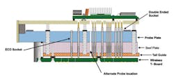
Wireless fixtures were introduced to address the limitations associated with long-wire fixtures. A multilayer PCB, called a translator board (T-Board), replaces the nest of signal wires. The T-Board is designed using typical fixture-build files (Figure 1).
Automated PCB design software routes copper traces to replace the signal wires. Double-ended probes connect the UUT to the T-Board. Wireless fixtures generally perform much more reliably than wired fixtures because PCB designers can intelligently control exactly how each trace is routed.
Duplicate fixtures perform nearly identically, and electrical parameters are very consistent because there are no moving wires. Wireless fixtures also exhibit better crosstalk, reflection, and noise characteristics, which are particularly beneficial in low-voltage applications.
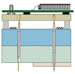
Cleaner signals permit the test to run at a faster rate, which allows the program of flash memory to run exponentially faster and even possibly at test-system speed. Internal fixture electronics are neater and more compact, reducing fixture height and saving space in the manufacturing environment. Small-scale ECOs are much easier to make even in high pin-count scenarios (Figure 2).
Advantages and Limitations
The advantage of wireless fixtures in contacting small targets bears further explanation. Wired fixtures allow the probe/socket to have a certain amount of misalignment between the socket's crush ring and its mounting hole. This can result in the probe/socket not being mounted perpendicular to the fixture and lead to missing small targets, resulting in a higher false failure rate.
Wireless fixtures can improve probing accuracy since any misalignment of the probe/socket is reduced by the tail guide plate. The tail guide helps center the socket during insertion and before the crush ring enters its mounting hole, resulting in near-perfect perpendicularity.
Both the top and tail guide plates are funnel drilled slightly larger than the diameter of the probe shaft. When test fixtures are manufactured with this process, probes typically contact the inner two-thirds of the test pad.
Wireless fixtures do have a few limitations. Low probe-count and prototype boards may not be good candidates for wireless fixtures because it may take longer to recover the additional cost of the fixture. And there are other potential limitations: The wiring cannot be visually traced, it becomes complex to make more than 100 ECOs, and the heights of components on the bottom of the PCB are limited to less than 1.250 inches.
Upon further analysis with regard to prototype boards and the enhanced performance of wireless, it may prove quicker to rule out fixture anomalies and proceed to debugging the UUT for design issues. This approach may reduce the overall debug time.
Fixture Selection Criteria
Several factors should be considered when selecting among the three types of fixtures for specific applications. As a general rule, wireless fixtures are the best choice if the UUT has medium to very high node-count, low-voltage components, and sensitive signals or if it requires special circuitry or custom electronics installed to increase test coverage. At the same time, they provide the best reliability while keeping profile, weight, and maintenance to minimal levels.
Short-wire fixtures provide a good choice for stable and mature medium to high node-count UUTs. Although their signal fidelity is not equal to wireless fixtures, they are an alternative to long-wire fixtures. The weight, maintenance, and profile of short-wire fixtures are similar to wireless fixtures.
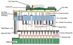
Long-wire fixtures historically have been used for all node-counts typically when price rather than test performance was a driving factor. While signal fidelity is limited, they are proven and reliable. Like their weight, their maintenance effort is higher (Figure 3).
Figure 3. Fixture Terminology
General Fixture Designs
In many respects, the best practices for the design and application of wireless fixtures are very similar to those for more conventional wired designs. Standard top plates should have a minimum thickness of 0.187 inch; contoured top plates, upon which the UUT is set directly, can range from 0.250 to 0.375 inch depending on the UUT topography. The top plate should be registered to the probe plate with at least three locking guide pins to align the top and probe plates.
Probe plate thickness for wireless fixtures varies from 0.500 inch to 0.562 inch depending on several factors including UUT characteristics, standard socketed or socketless probe type, and fixture size. The fixture vendor will select the correct thickness to maintain the desired probe contact force for each application.
Probe travel should be viewed differently now that the restriction of hazardous substances (RoHS) has introduced new parameters that will affect the manufacturing process. Contact force should be viewed as the new standard rather than probe travel since contact force at the probe tip is used to penetrate the flux and contaminants on the UUT.
Required contact pressure is dependent on the feature being contacted, surface finishes, and manufacturing processes. As a general rule, 4 to 8 ounces of contact force are necessary for test pads, vias, and leaded devices for no-clean, lead-free solders.
Guided probe technology is recommended for fixtures contacting test pads below 0.028 inch in diameter. Two diagonally opposed tooling pins should be installed in the guide plate for accurate UUT to bed-of-nails registration. A clear observation plate with the same thickness and dimensions as the UUT will keep the probes clean when the fixture is not in use.
Selecting the Best Actuation Method
Three main methods reliably engage the board under test to the bed-of-nails in the test fixture:
Vacuum Actuation
Vacuum actuation, the industry standard, is lightweight and reliable for applications up to 6,500 nodes. These versatile fixtures allow dual-sided and dual-stage probing as well as the use of side-probing features. Wireless versions also are available for most major test platforms.
Pneumatic Actuation
Pneumatic actuation provides a very balanced and controlled distribution of pressure, resulting in more reliable contact to test pads as small as 0.012 inch. The speed of actuation and retraction as well as timing can be controlled, allowing specialized tests to be performed. Dual-sided and multilevel probing is easily accomplished.
Pneumatic fixtures provide a very robust platform for engaging boards and connectors, and increasing test coverage to nets that may not otherwise be available by probe. These fixtures typically are reserved for more complex, higher-density circuit boards that require more thorough testing. Due to their nature, these fixtures will tip the scale more aggressively than their vacuum counterparts. Again, wireless options are available for most major test platforms.
Board Handlers
Board handlers can vary greatly by manufacturer so it is difficult to make statements that apply to all. Some board-handler fixtures can be less expensive since actuation methods do not have to be incorporated into every fixture.
But, there are several disadvantages to consider. A substantial one-time investment is involved to acquire the board handler itself. Also, the migration path to other fixturing methods or other manufacturing facilities can be difficult or even impossible.
This is a good choice for high-volume products with test-pad diameters no less than 0.030 inch. Complex testing and wireless options are limited. Pricing and weight of the fixtures will vary depending on the handler type.
Special Design Considerations
Some additional design considerations apply particularly to wireless fixtures, such as the need to probe tall connectors on the bottom of the UUT. Typically, probing connectors more than 0.200 inch tall requires a more customized approach when using a wireless fixture.
Today's test engineers are more familiar with PCB design, so the growing trend toward wireless fixtures gives them an opportunity to influence T-Board design. Often, the customer provides very valuable design input such as calling out potential aggressor or victim signals that need to be isolated.
In one particular case, a customer had a board with many signals requiring isolation. The customer worked closely with the T-Board designers to configure the shielding layers and ground planes to meet the stringent test requirements. Thanks in part to the customer's input, the T-board met every requirement.
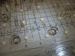
Wireless fixtures enable a unique method of implementing ECOs (Figure 4). Each wireless fixture is designed with up to 100 ECO sockets spaced around the perimeter of the UUT, which are connected to the tester's open resources. A new test point can be added by installing a socket and probe from the top and wiring the socket to an ECO location on top of the probe plate.
This method is much easier than making a change to other fixture designs since there is no wire mass making it difficult to drill, load, or wire the sockets. The result is a substantial time-savings for ECOs. Even if a new probe location needs to be added to the fixture, often it is not necessary to remove the T-Board.
Economics of Fixture Design
The capability of wireless fixtures to handle large numbers of nodes, particularly numbers >7,000, provides the potential for using a one-board, one-tester, one-fixture approach. In some applications, it is possible to replace two ICT systems with one, reducing capital equipment, labor, maintenance, and floor-space costs.
In cases where an ICT system is used and fixtures are changed for each UUT, the beat rate can be cut in half and labor costs substantially reduced by eliminating the need to change the fixture. Test-development time also can be substantially reduced because only one program needs to be developed for each board.
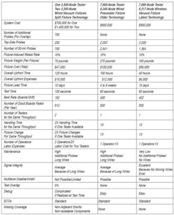
Table 1 documents a typical example of the substantial economic benefits wireless fixturing technology can provide when using the one-tester, one-fixture approach. This study compares three different fixturing methods on a 5,700-node board. The three methods include a 3,500-node tester with two 3,200-node long-wire fixtures using split fixture technology, a 7,680-node tester with a 6,246-node long-wire pneumatic fixture, and a 7,680-node tester with a wireless vacuum fixture.
The table shows the disadvantages of testing a board with two fixtures. Although the cost of building the fixture is approximately the same whether one or two fixtures are used, the up-front costs involved in designing two fixtures are less with a single long-wire fixture than two long-wire fixtures and much less with a single wireless fixture. This is because long-wire fixtures require a time-consuming manual effort to decide where to place probes on each fixture while the wireless process can be performed using PCB routing software.
The figures in the case study assume that a single tester could be used for both the one-fixture and two-fixture approaches. In reality, if the process involved a faster beat rate than could be accomplished by changing fixtures, then two testers would be required for the two-fixture approach. If only one tester is used with two fixtures, then the beat rate for the multiple fixture approach is only 182 boards per shift, less than half the beat rate for the one-tester, one-fixture approach.
To achieve approximately the same throughput using the multiple fixture approach, it would be necessary to invest in another tester. This would involve an additional capital expenditure as well as continuing labor costs.
Also by necessity, the multiple fixture approach involves considerable test overlap. The result is higher test time 100 seconds as opposed to 60 seconds for the single wireless fixture approach in this example which means lower beat rates and wasted capacity throughout the rest of the assembly process. The multiple fixture approach also requires approximately 700 additional probes in this example, which means higher initial costs and higher maintenance costs.
Finally, using the multiple fixture method, it is impossible to control and isolate many components, leading, for example, to the inability to test for nonadjacent shorts. By the same token, the multiple fixture approach cannot be used for multiple-level disabling or inhibiting.
On the other hand, the single-tester, single-fixture approach provides accessibility to all components and enables multiple-level testing. In this way, it supplies the maximum capability to prevent defects from escaping into the field where they can generate repair and recall expenses.
Acknowledgement
Figures 1, 2, 3, and 4 are courtesy of Joel Dirnberger at Circuit Check.
About the Authors
Michael J. Smith is a technologist for Teradyne's Assembly Test Division. He has more than 25 years of experience in test, inspection, and electronic manufacturing and has chaired the International Electronics Manufacturing Initiative Test and Inspection technical working group. Mr. Smith is an M.I.E.E. with a BSc in engineering from Leicester University. Teradyne, 600 Riverpark Dr., NR6002-17, North Reading, MA 01864, 800-837-2396, e-mail: [email protected]
Neil Adams is a product manager at Circuit Check. He has more than 22 years experience in the ATE fixture design and fabrication industry. Circuit Check, 6550 Wedgwood Rd., Maple Grove, MN 55311, 763-694-4214, e-mail: [email protected]
