System-level test, extreme ultraviolet (EUV), 450-mm wafers, 3-D ICs, MEMS, inspection tools, and modular instruments for IC test are key areas of semiconductor industry focus, based on exhibits at the recent Semicon West trade show and presentations at the co-located Test Vision 2020 workshop.
Karen Savala, president of SEMI Americas, specifically cited 3-D IC packaging, EUV lithography, and 450-mm wafers as important areas of investigation for moving Moore’s law ahead as she introduced keynote speaker Shekhar Y. Borkar, an Intel fellow and director of extreme-scale technologies. For his part, Borkar described himself not as a process technologist but a “happy user” of the technologies such as the ones Savala enumerated. “I will exploit [those technologies] to make computing ubiquitous,” he said.1
Organizations working on technologies that Borkar can exploit range from research labs to providers of general-purpose modular instruments with semiconductor test applications. In the former category, Imec announced the Flemish government’s intention to invest in building the company’s 450-mm cleanroom facilities. With the combination of a 300-mm cleanroom and the transition to 450-mm, Imec will be able to keep delivering its partners research on sub-10-nm devices, enabling the future growth of the global nanoelectronics industry, the organization reported.
Imec said it already is setting up collaborations on the 450-mm transition, with an early initiative involving the installation of Surfscan SP3 450, a 450-mm-capable wafer-defect inspection system from KLA-Tencor. “This tool will be essential to detect ultra-small defects, which have a substantial impact on yield when scaling to the sub-10-nm technology nodes,” said Luc Van den hove, president and CEO at Imec.
At the other end of the innovation gamut, providers of PXI instruments, including National Instruments (NI), Geotest, Pickering Interfaces, and ZTEC Instruments, showed products ranging from switch and RF instrument modules through complete test systems. NI, for example, touted its graphical system design platform coupled with PXI hardware to serve semiconductor applications. The company cited successful applications of the technology: TriQuint Semiconductor used LabVIEW and PXI modules to characterize RF power amplifiers; Fraunhofer ISIT employed a PXI platform to test MEMS inertial sensors; and Austriamicrosystems, in conjunction with the Automation Systems Department of the University of Applied Sciences (Graz, Austria), used a PXI-based automated system to characterize ADCs.2
The Test Vision Workshop
Participants in Test Vision 2020 focused on the future, with presenters forecasting the evolution of technology in system-level test (SLT), test efficiency, MEMS test, and 3-D IC and through-silicon-via (TSV) test.
Greg Smith of Teradyne offered a presentation on the practicality of eliminating SLT using protocol-aware ATE. He noted that SLT typically is the last test insertion before shipment, adding that test times can be minutes long and that SLT might be eliminated once functional test coverage is sufficiently high. He presented a hypothetical cost model that test engineers could use to evaluate the effectiveness of using ATE to perform SLT.
Steve Ledford of Advantest and Wes Smith of Galaxy Semiconductor teamed up to describe a data-driven approach to ATE overall equipment effectiveness (OEE). Their goal was to help fabless and IDM companies improve characterization efficiency, accelerate yield ramp, maximize wafer and final-test yield, and reduce test cost while maximizing throughput. For OSATs, their goal was to identify marginal test programs, minimize tester downtime, reduce retest, and decrease test-cell-related yield excursions.
Ledford and Smith described short-loop and long-loop approaches to process-control optimization. A short-loop control approach based on Advantest’s V93K platform could dynamically perform retests, generate alerts related to tester/handler issues, and maintain a list of sensitive tests. A Galaxy-based long-loop analysis step, employing the firm’s Examinator, could help identify sensitive tests, analyze tester-to-tester variations, analyze long-term trends, and generate alarms based on long-term trends.
Devin Morris of Roos Instruments also addressed test-data issues in a presentation titled “Moving Beyond STDF Log Files: Innovations for Navigating the Sea of Test Data.” He noted that STDF files have limited scope, and evaluating STDF data is a reactionary process: “By the time you know there is an issue, it’s a big issue.” He proposed a method of providing semantic information—metadata—in addition to quantitative metrics and correlations to automate the investigation process. The metadata provides for less data to handle, and it avoids sensitive or proprietary test-data restrictions.
Morris described a method of generating metadata based on the Roos Guru tool, which integrates the company’s Cassini software environment with a database and networking backbone. With cloud computing, the database could scale, and metadata could be accessed anywhere.
Handling MEMS and 3-D Stacks
Bernhard Lorenz of Multitest addressed both MEMS test and 3-D IC test in a presentation titled “Enabling Highly Parallel Sensor and SOC Test: Can Handling Equipment Keep Pace with ATE?” He noted that traditionally, ATE has been complex and expensive, with costs driven by requirements for more channels, power supplies, and analog resources; in contrast, the mostly mechanical handlers have represented only a small percentage of the overall test cell cost.
He noted, however, that handler capabilities must keep pace when it comes to supporting highly parallel SoC test. And MEMS devices will require actuation of up to nine degrees of freedom (DoF) in one insertion. Applying multiple stimuli at one insertion, he said, not only will provide the best cost of test but also ensure that test conditions most closely match those of the final real-world application.
Courtesy of Multitest
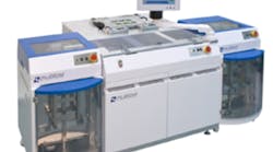
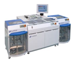
The move to 3-D ICs, he said, will require a variety of test steps: wafer-level tests to ensure known good dies (KGDs), partial-stack test to ensure good tested stacks, and final test to ensure good tested packages. Lorenz noted that handlers capable of supporting 3-D test applications are available today. In early July, Multitest introduced its Plug & Yield solution for the test of 3-D packages. The fully integrated setup consists of a Multitest InStrip3D (Figure 1), a test interface board, and a contacting solution based on vertical-spring technology. A customer will use the combination for electrical test of partial stacks during assembly of a mobile SoC.
Also addressing handlers for 3-D IC test was Zain Abadin of Advantest, who likened the challenge to balancing an elephant on a chip. To ensure high performance, he told workshop participants, you need to apply the weight of an elephant to your chip without causing damage. Challenges, he said, include higher DUT power dissipation, finer pin/pad pitches, and higher pin/pad counts. Advantest technologies that can help meet the challenges, he said, include soft-touch handling, which controls the force of impact during handling and ensures force balancing.
On the Semicon West exhibit floor, Abadin highlighted the development of a new product line of fully automated and integrated test and handling solutions for TSV-based 2.5-D and 3-D products. The company’s concept-model test cell, dubbed DIMENSION, integrates a high parallel test cluster along with singulated die and 3-D die stack automated handling capabilities.
New Products on Exhibit Floor
Courtesy of Geotest-Marvin Test Systems
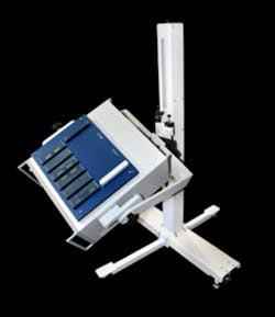
Specific new products on the exhibit floor ranged from sockets to complete systems. In the latter category, Geotest highlighted the expanded capabilities of its TS-900 platform, which now offers a new manipulator option (Figure 2) and an automated handler-compatible receiver. The Reid-Ashman OM1069 Manipulator is designed specifically for the TS-900 and allows precise positioning and flexibility for interfacing to automated probers and device handlers used for production testing of semiconductor devices. The manipulator’s spring-loaded design facilitates easy alignment and docking to handlers—eliminating the need for a complex receiver interface.
The TS-900 also features a new handler-compatible receiver, which offers the flexibility to interface to virtually any device handler. In addition, fixture compatibility is maintained with the TS-900’s current receiver, allowing users to interchange load boards between the screw-down and slide-receiver configurations.
Courtesy Aries Electronics
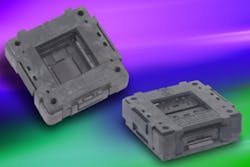
Aries Electronics announced that it now offers a top-load burn-in socket that saves significant time and money over conventional top-load sockets for new IC pin-out designs (Figure 3). With delivery in four weeks and tooling costs of only $200, the new top-load socket enables designers to reduce development and production costs that previously took up to three months and ran more than $30,000, according to National Sales Manager Paul Ruo. Based on a modular design, the new socket can be configured to accommodate devices on 0.3-mm pitch and higher, and it can be employed for virtually any SMT device, including BGA, µBGA, QFN, LGA, and bare dies as well as a number of other devices like those used for MEMS testing with high acceleration rates.
In addition to the time and cost savings, the new top-load socket helps reduce device damage for equipment under test by minimizing several points of over-compression and errors in device insertion. Devices are loaded and unloaded on the top of the socket without compressing the socket or holding it down. When engaged, the socket also avoids over-compression with pressure pads that cover a larger surface area to distribute force on the device. A built-in hard stop also reduces insertion force on the PCB.
The socket comes in a top-load configuration ready for device insertion so no special tooling or push plates are required. The manual dual latches can be removed to allow the socket to open when the force is removed for efficient and quick testing of multiple devices. These sockets are easy to mount and remove from the test board thanks to two specifically located stainless steel alignment pins that are extremely precise. The sockets’ relatively low cost and small overall size allow the maximum number of sockets per BIB (burn-in board) and BIBs per oven while remaining operator friendly.
The compression spring probes leave minimal witness marks on the bottom surface of the device pads for increased reliability. Compression spring probes are constructed of heat-treated beryllium-copper and plated with a minimum of 30 micro inches (0.75 micro mm) gold per MIL-G-45204 over a minimum of 30 micro inches (0.75 micro mm) nickel per SAE-AMS-QQ-N-290. Contact forces are 15g per contact on a 0.30 mm to <0.40 mm pitch, 16g per contact on a 0.40 mm to <0.50 mm pitch, and 25g per contact on pitches of 0.50 mm or larger. Estimated contact life is a minimum of 500,000 cycles, and the operating temperature is -55°C to +150°C. Pricing starts at $125, and delivery is 20 working days.
Benchtop SEM
JEOL introduced a new NeoScope scanning electron microscope (SEM), which offers higher magnification than the original NeoScope benchtop version introduced in 2008. The company reported that the original version has been used for inspection of electronic parts, forensics analysis, pharmaceutical inspection, and imaging insects for student projects. It also is applied in conjunction with both optical microscopes and traditional SEMs in the lab.
As simple to use as a digital camera, the NeoScope is a high-resolution SEM that produces images with a large depth of field at magnifications ranging from 10x to 60,000x. It features high and low vacuum operation, three selectable accelerating voltages, and secondary electron and backscattered electron imaging. The NeoScope accommodates samples up to 70 mm in diameter and 50 mm in thickness. Both conductive and nonconductive samples can be examined. Optional EDS (energy-dispersive X-ray spectroscopy) is available for elemental analysis.
An additional new feature of the NeoScope SEM is a touch-screen interface with the familiar look and feel of today’s smart phones and touch pads. Automatic functions as well as prestored recipe files make it easy to use for many sample types.
The company also said its new series of field-emission SEMs is complete with the recent introduction of the subnanometer imaging resolution JSM-7800F. JEOL’s highest performance FE-SEM makes it possible to observe the structural morphology of nanomaterials at 1,000,000x magnification with sub-1-nm resolution; perform low-kilovolt imaging and analysis of highly magnetic samples; collect large area EBSD maps at low magnifications without distortion; and image thin, electron transparent samples with sub-0.8-nm resolution using an optional retractable STEM detector.
References
1. Nelson, R., “Keynoter Describes Ubiquitous Computing from Data Center to Pacemaker,” EE-Evaluation Engineering, Rick’s Blog, July 10, 2012.
2. “Solutions for the Semiconductor Industry,” National Instruments, 2012.
For More Information
Advantest
Aries Electronics
Galaxy Semiconductor
Geotest-Marvin Test Systems
Imec
JEOL
Multitest
National Instruments
Pickering Interfaces
Reid-Ashman
Roos Instruments
Teradyne
MEMS Roadmapping to Address Test Challenges
As semiconductor technology extends into “more than Moore” territory, test engineers will need to contend with integrated devices containing multiple MEMS structures. A roadmap can be useful in establishing effective test strategies, according to Dr. Michael Gaitan of NIST, who delivered an invited address at the Test Vision 2020 workshop held in conjunction with Semicon West.
Gaitan, who chairs the iNEMI and ITRS MEMS technology working groups, said his intention was not to talk about solutions but rather problems. The interesting thing about roadmapping, he said, is the effort to find common ground. Consensus metrics arrived at by working groups, he said, are ones least objectionable to the range of companies working together.
A roadmap, Gaitan said, is a plan that matches goals with solutions. There are several problems with generating a roadmap, including settling on figures of merit and prompting companies to work together and share information. The semiconductor industry has settled on technology nodes as signs along its roadmap, but, said Gaitan, MEMS are too diverse, with different processes for each device, secret sauces from each manufacturer, and intense competition. To simplify the process, he said, participants decided to narrow the focus to MEMS technologies that will be part of a mobile Internet set of devices.
Gaitan suggested that, for inertial sensors, a roadmap might be based on degrees of freedom (DoF) at both the package and chip levels. As an example, he said integrated 10-DoF chip-level products might appear in 2017.
Grand challenges remain, he said, involving standardization of MEMS packages to support integration, identifying the role of wafer-level testing, establishing methodologies for design for test or design for no test, and gaining more knowledge of the physics of failure. He noted that today, device fabrication accounts for one-third of MEMS manufacturing cost while packaging and testing account for the other two-thirds.
In contrast, R&D investment in packaging and testing is miniscule in comparison to that in device and process development. “We know how to design devices, but we haven’t put a fair share of investment in the backend, and maybe we should do that,” he said.
Unfortunately, he said, there is little uniformity in reporting MEMS performance in device datasheets, an issue iNEMI is addressing. He noted that companies often develop custom test capabilities and train their own test engineers. MEMS sensor fusion will continue to create challenges for testing increasingly complex devices while lowering test costs. In addition, he said, tools are needed for DFT, BIST, and self-calibration.
“Our roadmapping so far is near-term—we are looking at incremental improvement in performance,” Gaitan said, with the near-term being five years or so. The concept of the integration node might facilitate longer term roadmapping of MEMS and other “more than Moore technologies,” he concluded.


