Vendors Explore Data-Capture Options
Sensor manufacturers continue to innovate as they introduce products that handle physical and biological measurement tasks. Meanwhile, data-acquisition-system and sensor-network vendors work to facilitate the capture and processing of the data the sensors collect.
One issue centers on where acquired data is processed and how. One entity addressing that issue is the IEEE P1451 Working Group (WG), which in September announced its intent to develop IEEE P1451.001 Recommended Practices for the Signal Treatment Applied to Smart Transducers. According to the WG organizers in their call for participation, “IEEE P1451.001 will define signal-processing algorithms and data structure to share and to infer the signal and state information of an instrumentation or control system.”
The goal is to develop algorithms that account for signal characteristics as well as characteristics of the transducers attached to the system, with the algorithms able to perform shape analysis in accordance with exponential, sinusoidal, impulsive-noise, noise, tendency, and related functions. The standard also will define commands for requesting information.
Organizers have invited participation from “…sensor and transducer manufacturers, data-acquisition vendors, sensor application developers, sensor system users, and system integrators in industrial, consumer, medical, health, environmental, and other relevant fields.”
A sampling of DAQ manufacturers suggests it’s premature to expect the dot 001 standard to have benefits for DAQ and sensor customers. Bob Judd, director of marketing at United Electronic Industries (UEI), said the company is not looking to implement special functions for smart sensors. In fact, he said, “We try to stay sensor-agnostic, and we’re happy to connect via old-fashion analog or serial port—Ethernet, CAN, or any other popular interface.”
He said he does see occasional requests for a transducer electronic datasheet (TEDS) interface, which is addressed in the older IEEE P1451.4 standard. UEI’s recent products include the DNx-AI-224, a four-channel, high-speed strain-gage input board; the DNx-IRIG-650, an IRIG and GPS timing interface; and the UEI-RSS Remote Serial Server Software for the company’s DNx-SL-501 and DNx-SL-508 serial cards.1
Shea Clymer is business development manager for sensors at National Instruments (NI), which has been instrumental in developing the TEDS standard. He commented on trends in the sensor industry, including ones related to TEDS and the types of processing that might be addressed in the new .001 standard. “If you think of our wireless sensor network (WSN) nodes, for instance—they connect to sensors and have an ADC inside them. They can do their own signal processing and then transfer data wirelessly to other computers. What we are doing may not necessarily conform to the .001 standard, but it benefits our customers now,” he said.
As for TEDS, Clymer explained, “TEDS is stable. The committee continues to meet but not with a sense of urgency with respect to meeting any deadlines.” In contrast, the efforts are aimed at refinements and updates.
The biggest issue with respect to dot 4, Clymer said, is adoption. “We continue to see adoption, which is good.” He commented on some impediments to adoption: “NI played a large role in spearheading the initiative, but it was up to the sensor vendors to implement it.” Currently, he said, “We’re developing closer partnerships with sensor vendors. We continue to promote and drive the standard with them as well as support it on our instrumentation, and we are hearing more and more questions about support for TEDS.”
Initially, he said, TEDS focused on accelerometers, but now he is seeing interest with respect to microphones. Further, he noted, in the structural test world, he has seen Boeing adopt standards for TEDS to implement strain-gage systems. Boeing, he said, is doing some custom work to embed TEDS chips inside connectors.
Further, he said, there are situations in which engineers don’t need TEDS for all their applications. “It really becomes useful when you have a large number of sensors within your organization, and you need tracking calibration” for each individual sensor. And, he said, “It’s nice to have if you have a lot of sensors on a structure—then, during the test, it helps you identify the health of sensors and where they are located.” On the other hand, “For the engineers who don’t have a large test-and-measurement component to their organization—engineers testing a widget in the lab—TEDS doesn’t add as much value.”
Clymer said that there is a trend toward bringing more signal processing down to the sensor level. He cited as an example a new USB sensor system from DYTRAN, which acquires accelerometer and temperature data.
DYTRAN describes the system, which it calls the 5340 USB Vibration Measurement System, as a combination of its 7543 USB Accelerometer, VibraScout Software Application, and VibraScout Post Processor Software. The 7543A is a USB-powered device that allows for real-time, three-directional acceleration acquisition along with temperature-data and pitch/roll-data acquisition. Built-in firmware handles USB communications and provides for storage of the device serial number, storage of accelerometer and temperature calibration data, and additional storage for customer information, such as last calibration date. 2
Clymer at NI said he has heard of many sensor companies wanting to continually push more of the processing toward the sensor level. With MEMS sensors in particular, companies want to take advantage of the processing power available on the sensor. Nevertheless, Clymer said, there are some questions about the benefits of standardization and even whether something might be lost by performing processing at the sensor. It might make sense, he said, to hand off the processing to a node farther back from the sensor, where that node, interfacing perhaps with several other sensors, can provide benefits through a more synchronized form of data processing.
Since EE-Evaluation Engineering’s last looks at wireless sensor networks3 and the sensors themselves,4 innovation has proceeded on both fronts.
WSN Innovations
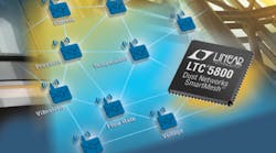
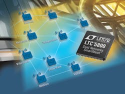
With respect to WSN, in October Linear Technology’s Dust Networks product group introduced the SmartMesh LTC5800 (system-on-chip [SoC]) and LTP5900 (module) families, which the company claims are the industry’s lowest power IEEE 802.15.4E-compliant WSN products (Figure 1). SmartMesh ICs and modules enable tiny sensor “motes” to be designed with a battery life of more than 10 years while companion network-manager components support the development of robust and secure WSNs.
Courtesy of Linear Technology
SmartMesh networks use what Dust calls a “triple play” of wireless mesh technologies—time diversity, frequency diversity, and physical diversity—to assure reliability, resiliency, scalability, power-source flexibility, and ease of use. At the core of this technology is an intelligent mesh network with advanced algorithms and power-saving technologies that enable features unavailable from other WSN providers. These include deterministic power management and optimization, auto-forming and self-healing mesh technology, zero-collision low-power packet exchange, and scalability to large, dense, deep networks.
Two communications standards are supported: the SmartMesh IP version is compliant with the 6LoWPAN standard, providing native IPv6 addressability to every node. The new SmartMesh WirelessHART IEC62591-compliant products double the battery life over the prior release.
The SmartMesh family consists of several products to simplify system development. The LTC5800 SoC includes robust sensor networking software in a 72-pin 10-mm x 10-mm QFN package. The LTC5800 integrates all radio circuitry components, including an onboard power amplifier and an ARM Cortex M3 32-bit microprocessor, requiring only power, ground, and an antenna for robust wireless connectivity. The LTP5901/LTP5902 mote modules provide a surface-mount PCB that has undergone FCC, CE, and IC modular radio certifications. The LTP5901 module includes an onboard chip antenna while the LTP5902 module features an MMCX antenna connector.
Joy Weiss, president of Linear Technology’s Dust Networks product group, stated in a press release, “Our primary goal is to enable our customers to confidently place sensors anywhere data needs to be gleaned. The advent of SmartMesh WirelessHART systems and the addition of IP-enabled wireless sensor networks reflect Linear Technology’s continued commitment to that goal.”
The Dust announcement was accompanied by two quotes from customers. Bob Karschnia, vice president, wireless, for Emerson Process Management and business leader of its SmartWireless product line, stated, “Dust Networks is unique in its focus on simultaneously delivering ultralow-power and reliable wireless networks. We have more than 1 billion hours of successful operation of Emerson’s SmartWireless instruments in the field utilizing Dust Networks’ SmartMesh WirelessHART components. We are excited about the promise of the LTC5800, providing twice the battery life and enabling new applications within the industrial process market.”
Also, Mark Housley, CEO of Vigilent, stated, “The data-center environment is extremely harsh to RF, and our customers demand that our energy-management and data-center analytics systems are deployed with minimum disruption to the data center. Dust Networks-based wireless sensors help ensure that Vigilent technology will continue to deliver solutions for mission-critical facilities with no impact on data-center operations.”
Linear said SmartMesh WirelessHART was purpose built to serve the low-power and reliability requirements of the industrial process market. These attributes serve the needs of many diverse applications, and SmartMesh IP maintains comparable performance while adhering to the 6LoWPAN standard.
In addition, Professor Steven Glaser with University of California, Berkeley is responsible for the sierranet program, which enables measurement of temperature, humidity, snow depth, soil moisture, and solar radiation levels in remote environments using SmartMesh-enabled sensors. He stated, “Our goal is to provide accurate, remote environmental monitoring to track the status of California’s water supply. With a SmartMesh IP IPv6 routing node able to run at under 50-µA average power consumption, SmartMesh IP represents a new paradigm for sensor networking, combining the ease of web programming with the long life and reliability of Dust Networks’ industrial products.”
All SmartMesh networks are centrally managed, which provides comprehensive security and network management capabilities. The SmartMesh WirelessHART manager (LTP5903) can support up to 500 nodes per network, SmartMesh IP managers can accommodate up to 100 nodes per network, and multiple instances of SmartMesh subnetworks can be deployed side-by-side to create very large networks.
Sensor Sampling
Among other sensor announcements, Analog Devices introduced a MEMS accelerometer with min/max offset sensitivity over the full temperature range. The ADXL350 three-axis MEMS accelerometer has maximum offset temperature sensitivity of ±0.31 mg/°C on the X/Y axes and ±0.49 mg/°C on the Z axis, guaranteeing predictable performance across the full temperature range of -40°C to +85°C. The ADXL350 Min/Max offset sensitivities guarantee known, quantifiable offset sensor measurements even in applications that are subjected to a wide temperature range. Additionally, the ADXL350 offers low noise density enabling designers to obtain valid measurements from applications with a low noise floor.
Biosensors, too, got some attention as Tokyo Electron (TEL) and imec announced in October the participation of TEL in imec’s Human++ bio-research program. The agreement includes collaboration on biosensors and specialty imaging.
One of the research tracks within imec’s Human++ program is the development of next-generation platforms for automated cell-inspection methods to create pluripotent stem cells in clinical grade. The agreement between TEL and imec includes the development of high-quality imagers and sensors for a platform for inspection of Induced Pluripotent Stem Cells (IPSCs). A compact lens-free imager will be developed at imec to monitor IPSC colonies, and imec will design a silicon photonics biosensor to quantify biomolecules involved in stem-cell proliferation.
To further strengthen their collaboration, TEL will participate in imec’s resident researcher program and send, for the first time, a researcher to imec for joint research in the life science field.
“By participating in imec’s Human++ program, TEL believes it will be possible to apply the technological strengths and expertise—both tangible and intangible—it has gained in the semiconductor production equipment business to the life science field. imec’s extensive multidisciplinary track record is expected to be the ideal breeding ground to develop new technologies supporting next-generation life science solutions,” said Yoshio Kinoshita of TEL, in a press release. “Moreover, imec’s unique environment of a semiconductor cleanroom combined with biolabs and a multidisciplinary team of engineers, physicists, and biomedical and chemical scientists allows in-house cultivation of stem-cell colonies, biochemistry development, and in-house testing with biological molecules and stem-cell colonies.”
“imec’s vision on future healthcare is one of high-quality and affordable diagnosis and treatment. We want to advance that vision by providing innovative electronics solutions to our partners,” said Peter Peumans, director of the life sciences program at imec. “I am delighted with this new agreement, broadening our collaboration scope with TEL from semiconductor technologies to life sciences. This collaboration endorses our expertise in life sciences and the value of our offering to TEL throughout our long-term strategic collaboration in the framework of imec’s advanced lithography affiliation program.”
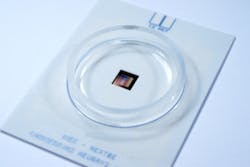
imec’s technology includes a CMOS chip with a matrix of micronails with various dimensions, packaged in a dish suitable for cell cultures (Figure 2). With these micronail electrodes, individual cells can be stimulated and recorded. The organization said that the platform—with its two-way stimulus and response electrical-communications capability—can serve as an instrument that supports research on in-vitro cell cultures and that it could aid, for example, in Alzheimer research and drug development projects.
Courtesy of imec
References
1. Nelson, R., “DAQ Technologies Support Broad Measurement Range,” EE-Evaluation Engineering, May 2012.
2. 5340 USB Vibration Measurement System, DYTRAN Instruments, Preliminary Operating Guide, July 13, 2012.
3. Nelson, R., “Collecting Data at the Edge,” EE-Evaluation Engineering, March 2012.
4. Nelson, R., “From Images to Movement, Devices Catch Data,” EE-Evaluation Engineering, January 2012.
For Further Reading
- Johnson, T., ”HART Communication Networks Are Improved by Small, Flexible, Low-Power Modem ICs,” Analog Dialogue, Volume 46, October 2012.
- Laplace, P., Ph.D., University of Nevada Researchers Use LabVIEW, PXI, and CompactRIO to Measure the Effects of Earthquakes on Bridges, National Instruments, Case Study.


