Inspecting Mounted Components and Bare Boards Acoustically
When an electronic component is being inspected by an acoustic microscope, ultrasound is pulsed into the part by the scanning transducer. At any material interface within the part, a portion of the ultrasound that has been pulsed into the part is reflected as an echo signal while the remainder travels deeper. Using the echo signals to create an acoustic image is known as reflection-mode imaging. Using the ultrasound that exits the far side of the part is known as transmission-mode imaging.
A great deal of acoustic imaging is performed on trays of components before assembly and before reflow. This typically is reflection-mode imaging. The return echoes can be, and generally are, gated on a depth of interest. The precise amplitude of the signal, the shade of gray, and the polarity of the signal that will appear in the acoustic image can be calculated from the physical properties of the two materials—epoxy and silicon, for example.
The purpose of this type of reflection-mode imaging is to find and remove from an assembly those components having gap-type internal defects because the defects can, by thermal cycle-induced expansion, corrosion, or both mechanisms, break electrical connections. The parts being imaged often are plastic-encapsulated microcircuits but also may be ceramic IC packages, ceramic chip capacitors, or the board itself. The defects are gaps containing air or another nonsolid, and the gap, even if no thicker than 0.01 micron, has two material interfaces. The top interface reflects >99.99% of the ultrasound and, unlike other internal features, appears bright white in the acoustic image.
This role of acoustic imaging in screening loose components, or in failure analysis, is well known, but there are two other applications that also contribute, directly or indirectly, to overall reliability: the reflection-mode imaging of mounted components after reflow and the transmission-mode imaging of bare boards.
Imaging Surface-Mounted Components
When a populated PCB has gone through reflow and subsequently fails life tests, acoustic imaging of the surface-mounted components often is performed in an attempt to learn, nondestructively, what caused the failure. Typically, boards fail because of a broken connection. If the broken connection is in a via or trace inside the board, imaging of the mounted components will not find it. Nor will it find a defect that involves only on-chip circuitry. But it will find the very frequent connection-breaking structural defects within the component package.
The technique for imaging the components surface mounted onto a board is quite different from the technique for imaging a tray of components. In a tray, all of the components are of the same size and in the same horizontal plane. When the transducer sends a pulse of ultrasound into a component, return echo signals come back from the material interfaces, including gap interfaces, at all depths. Usually the returning echoes are gated on (limited to) a specific depth of interest; for example, the mold compound-to-die face interface on parts that have a history of die face delaminations.
But on the board, the components include plastic IC packages, a mix of capacitors, resistors, transformers, connectors, and other items of various heights. The board’s side-view profile is far from flat. Since the transducer needs to scan back and forth, it must move in a plane higher than the tallest component. Clearance can be achieved by using a transducer with a longer focal length, such as a 50-MHz transducer having a focal length of 1.25 inches instead of the more usual 0.25 inch. Some image resolution will be lost because of the different characteristics of the transducer.
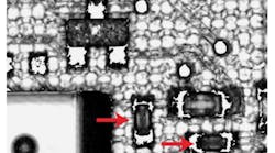
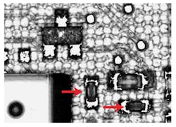
Figure 1 is the acoustic image of several components on a PCB. The purpose of imaging was to make visible defects in the two ceramic chip capacitors marked by the arrows in the lower right corner of the figure. The return echoes were gated on the depth of these capacitors, which are lower in profile than other components. As a result, the large component partly visible to the left of the capacitors is outside of the gate, as is the three-leaded component above it. The echoes for these components arrive at different times from the capacitor echoes and would have to be gated differently to display significant information. Because of the lower profile of the capacitors, however, gating on the internal structure of the capacitors corresponds to the weave pattern in the board as well as traces and vias.
Figure 1. Acoustic Image of PCB
Acoustic imaging captured the board surface weave and other details because the items of interest (capacitors marked by arrows) have a low profile. Images of larger, higher components have no significant data.
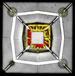
The components imaged on the board surface may be essentially unchanged from their pre-mount condition, or they may have been altered by reflow. The thin quad flat pack (TQFP) in Figure 2 was imaged after reflow. The surrounding board surface detail was not included in the imaging process. It is evident that reflow has caused extensive delamination of the die paddle from the mold compound (red and, where partly obscured by wires, yellow). At a minimum, the image indicates a reasonable risk that during service the delamination could lead to an electrical failure. In fact, the component may already have failed electrically.
Figure 2. Surface-Mounted TQFP
This surface-mounted TQFP has suffered internal delaminations (red, yellow) during reflow.
A component loose in a tray can be flipped over if there may be, for instance, a delamination at the back of the die paddle. The same component can’t be imaged from the back side after it has been surface mounted. A delamination between the back side of the die paddle and the mold compound is probably innocuous, but a crack running from the back side to the exterior is an open pathway for moisture and contaminants to enter the package—and it is not visible optically or acoustically from above after reflow.
Experience in Sonoscan’s SonoLabs suggests that few defects seen in components imaged on the board are the result of handling during assembly. A portion of the defects seen acoustically was formed during manufacture of the component; another portion was formed by reflow. Reflow-related defects are probably slightly less frequent than manufacturing-related defects.
The advantage of imaging a populated board is that rework can replace components that were found acoustically to have structural defects. This method saves boards that otherwise would be scrapped. It can be used on boards having large X-Y dimensions by using a Sonoscan imaging system that handles boards measuring up to 33 inches x 29 inches.
Imaging Bare Boards
The imaging of bare boards is largely carried out by board manufacturers as part of reliability testing for new products. A sample lot of boards is built, imaged acoustically, put through simulated reflow, and imaged again to determine the location and size of any defects that may have occurred during reflow.
Imaging is carried out using the Thru-Scan technique, where ultrasound is pulsed into the top surface of the board and received by a separate detector beneath the board. Technically, this method uses transmission-mode imaging where the ultrasound is transmitted through the entire thickness of the board; reflection-mode imaging collects echoes from various depths. In Thru-Scan, the transducer and sensor are both mounted on a C-shaped arm that performs the scanning. (The same technique is used on trays of components when it is desirable to know simply that a gap-type defect exists within the component without seeing fine detail or gathering depth information about a defect.)
The ultrasonic frequencies employed are low because they give better penetration; PCBs typically are harder to penetrate than components. A PCB consists of far too many layers and material interfaces for reflection-mode imaging, and some of the interfaces, such as copper to FR4, involve combinations of materials that reflect a high portion of the pulse.
Despite this, quite thick boards can be imaged. The thickness limit for a given board depends on several factors, including the type of resin; the type of filler; the filler to resin proportion; the number, thickness, and location of copper layers; and the manufacturing technology. The frequencies range from 10 MHz to 30 MHz (and occasionally, on a very thin board, to 50 MHz). Because the frequency is low, tiny defects are not imaged. The goal is to image gross defects such as delaminations that could impact long-term reliability.
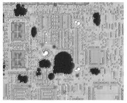
Figure 3 shows one portion of a transmission image made from signal amplitude data collected at each X-Y location. The texture of the weave at the board surface, seen in the reflection-mode image in Figure 1, is not visible in this image because it is simply one of many interfaces that the pulse travels through. Vias, bond pads, and other features are all visible here, but the significant features are the large irregular black features that indicate gap-type defects. The defects are actually imaged as acoustic shadows; that is, the gaps prevented any ultrasound from reaching the detector in these regions.
Pulsing ultrasound through a bare board and collecting arriving signals on the far side revealed vias, bond pads, and traces plus large internal gaps (irregular black regions).
On occasion, transmission imaging is used on populated boards. Over much or even most of the area of the populated board, transmission will be blocked by mounted components of various types. But when it is desirable to gain the maximum possible data about a failed board nondestructively, transmission imaging is worth the effort. If there are significant areas of defects, their black acoustic shadows may be visible in open areas between components.
About the Author
Tom Adams is a freelance writer and photographer who has written more than 500 articles for semiconductor and microelectronics trade magazines.


