Inspection systems address ‘middle-end’ semiconductor processes
Packaging advances are driving innovation at KLA-Tencor, which in May announced two new systems that support advanced semiconductor packaging technologies: CIRCL-AP and ICOS T830. Designed for characterization and monitoring of the diverse processes used in wafer-level packaging, CIRCL-AP enables all-surface wafer defect inspection, review, and metrology at high throughput. The ICOS T830 provides fully automated optical inspection of IC packages, leveraging high sensitivity with 2D and 3D measurements to determine final package quality for a range of device types and sizes. Both systems help IC manufacturers and outsourced semiconductor assembly and test (OSAT) facilities address challenges such as finer feature sizes and tighter pitch requirements as they adopt innovative packaging techniques.
In a recent phone interview, Prashant Aji, head of marketing for the company’s SWIFT division, commented on packaging trends. Driven by mobile devices, he said, packages are shrinking, with an increasing use of wafer-level packaging, and the industry is pushing to cut packaging costs. In addition, packaging is increasingly shifting to OSAT companies.
These trends are altering the semiconductor manufacturing process. With traditional packaging, Aji said, a silicon wafer undergoes wafer-level front-end processing, with wafer dicing and packaging occurring at the back end. KLA-Tencor addresses both these areas, having entered the back-end market in 2008 with the acquisition of ICOS.
But the move to wafer-level packaging, Aji said, inserts between the front end and the back end a new middle-of-the-line or “middle-end” stage, involving wafer-level through-silicon via (TSV), electrical redistribution layer (RDL), and bumping operations, with bump size and pitch decreasing, RDL line/space shrinking, and use of TSVs increasing. In addition, Pieter Vandewalle, senior director of marketing for KLA-Tencor’s ICOS Division, said that demands for longer battery life in mobile devices means less space for packages.
As a consequence, demand for advanced packaging inspection equipment is growing. Aji cited a Yole Déveolppment forecast that the market for inspection and metrology equipment for 3D IC packaging would increase at an 18% CAGR through 2019.
Courtesy of KLA-Tencor
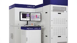
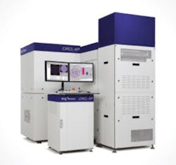
CIRCL-AP (derived from Concurrent Inspection and Review Cluster) addresses advanced packaging areas, supporting all-surface wafer inspection with up to 0.5-μm sensitivity (Figure 1). It performs front-side inspection and review, 2D and 3D metrology, and edge inspection and metrology.
It includes multiple modules that utilize parallel data collection for fast, cost-efficient process control of advanced wafer-level packaging processes. It supports a range of packaging technologies, including wafer-level chip-scale packaging, fan-out wafer-level packaging, and 2.5-D/3D IC integration using TSVs. The company’s 8-Series front-side inspection system serves as the CIRCL-AP’s front-side defect inspection and metrology module, which couples high-brightness LED scanning technology with automated defect binning to reduce nuisance problems and to speed detection of critical packaging defects, such as TSV cracks and RDL shorts.
CIRCL-AP’s CV350i module, based on KLA-Tencor’s VisEdge technology, enables detection, binning, and automated review of wafer-edge defects and metrology for critical edge trim and bonding steps in the TSV process flow. With multiple imaging and illumination modes, the Micro300 module can produce high- precision 2D and 3D metrology for bump, redistribution, and TSV processes. Utilizing a flexible architecture, the CIRCL-AP can be configured with one or more modules to address the requirements of specific packaging applications while the handler supports bonded, thinned, and warped substrates.
Vandewalle of the ICOS division emphasized that packages are evolving toward thinner devices, increasing demands for package height metrology and bare-die inspection. And cost pressures are driving a cost-of-ownership reduction. Next-generation packaging, he said, involves package-on-package (including a bottom logic chip and top memory chip), fanout WLP, flip-chip, BGA, LGA, and other configurations.
Courtesy of KLA-Tencor
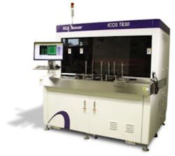
To address next-generation packaging, he said, the ICOS T830 combines four inspection stations and a sorting station in one system (Figure 2). It offers top, bottom, and side inspection modes and can detect voids, exposed copper, and other surface defects. It performs 2D package visual inspection to look for die cracks, and it employs 3D techniques for component-height measurement, ball inspection and metrology, and lead and pad inspection and metrology. It also performs resistor and capacitor 3D metrology.
ICOS T830 incorporates xPVI enhanced package visual inspection capability that enables high sensitivity detection of top and bottom component surface defects, such as voids, scratches, pits, chips, and exposed wires. The xCrack+ inspection station enables accurate detection of micro-crack defects—a key failure mechanism of thinner components used in mobile applications.
“Advanced packaging is undergoing significant technology changes,” Vandewalle said, with feature sizes shrinking and high-aspect-ratio structures requiring high sensitivity and throughput. KLA-Tencor, he concluded, is equipped to help packaging facilities meet the challenges.


