Matched tools for acoustic micro-imaging
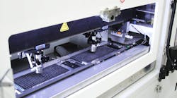
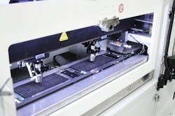
The capability of acoustic microscopes to image and analyze internal features, including structural defects, recently has been enhanced by technology that puts any number of acoustic microscopes in any number of locations on the same page. Send a part such as a plastic-encapsulated integrated circuit to any of your company’s plants around the world. Send with it the recipe for imaging the part—the ultrasonic frequency to use, the focal length of the transducer that pulses the ultrasound, and other parameters—and you will receive back the identical acoustic image from the personnel at each of your plants, even though they may be in different countries and speak different languages. Sonoscan developed the concept and calls it Globally Matched Tools (GMT) (Figure 1).
GMT permits engineers receiving acoustic images and data from multiple locations or multiple microscopes to be certain that the images and data are truly comparable, that the manufacturing processes are in good control, and that the results of applying the company’s accept/reject criteria are identical at all locations.
Tool matching has become common in recent years for instruments that perform optical and electrical inspection. The goal is to make their output data comparable at multiple locations and provide users with the assurance that a reported measurement of 50 microns is, in fact, 50 microns or that 210 millivolts is truly 210 millivolts.
Under the hood
The targets of acoustic imaging are gap-type defects such as voids, delaminations, cracks, and nonbonds as well as nongap defects such as tilted elements within the part. The ultrasonic pulse sent out by the transducer must travel through water that couples it to the sample. When a 100-MHz transducer sends a pulse of ultrasound into a part, the pulse actually consists of a range of frequencies from below 70 MHz to above 120 MHz. The echoes returned by a material interface will be somewhat differently distributed along a roughly similar continuum. These and other details made the development of tool matching for acoustic microscopes a challenging business.
Ultrasonic transducers for acoustic micro-imaging tools come in many frequencies, ranging from 5 MHz (good penetration but low resolution in the acoustic image) to 400 MHz (slight penetration but superb resolution). A common midrange transducer is 100 MHz—but transducers of this frequency are made with a variety of focal lengths and other characteristics.
The sensitivity of an acoustic microscope’s ultrasound to internal interfaces is extreme. A pulse of ultrasound that encounters a gap (filled with air, another gas, or a vacuum) will be reflected at virtually 100% even if the gap is as thin as 100 Å. Such a gap, or even a much thicker gap, is invisible to X-ray because the amount of missing material (if any) is minuscule. If the interface is the bond between two solids, the echo’s amplitude (20% perhaps, or 50%, but not near 100%) can be calculated by knowing the physical characteristics of the two solids—plastic and silicon, for example.
An experienced acoustic microscope user working in a laboratory can employ various techniques and alternate imaging modes to coax a meaningful image out of a difficult sample—for example, one that has multiple layers and therefore weak echoes. But in production environments, chip makers need a reasonably fast method to image a part, or thousands of parts, with absolute reproducibility—meaning that the acoustic microscope in Manila will produce, from the same part or tray of parts, the same acoustic image as the acoustic microscope in Arizona.
What Sonoscan researchers produced was the first calibration system that permits the matching of the operating parameters of multiple acoustic micro-imaging tools. It can match the two or more transducers, pulsers, receivers, and control electronics systems on a multiple-transducer microscope or large numbers of microscopes in multiple geographic locations. The same recipe is used for each part type for each of the identically configured imaging tools. Before imaging of the component begins, the calibration software tests the characteristics and performance of the transducer in numerous areas. If the transducer deviates from the required standards in any area, the acoustic microscope’s control software will refuse to use that transducer.
Tool matching
Development of the calibration system was a multi-year project that benefited from the company’s background. Sonoscan designs and manufactures all the components—transducer, pulser, receiver, and control electronics—in the ultrasonic chain. This means that the company can be sure that two or more transducers of a given frequency are designed to have the same operating characteristics, which in turn makes tool matching a more precise process. Tool matching would be difficult or impossible to achieve using commercial off-the-shelf transducers whose performance characteristics may vary in unknown ways and may drift over time.
Typically, a quality assurance or reliability group within a company will write the recipe of parameters to image a specific part type. A recipe usually looks at specific areas of interest within the part. The completed recipe is installed in every acoustic micro-imaging tool either directly or through the Internet. Use of the recipe ensures that all groups running the parts will obtain consistent results. The results do not depend on the functioning of an individual tool.
This methodology is essentially the reverse of most inspection routines where a sample part or tray of parts is imaged on a single acoustic micro-imaging tool, and the acoustic images then are examined to determine what the imaging parameters should be. Where anomalies can be subtle—in flip chips, for example—the imaging parameters devised by two groups running identical acoustic micro-imaging systems may be dramatically different because of the operators’ preferences or previous experience.
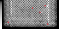
The flip chip imaged acoustically in Figure 2 has several anomalies and defects, some of which are marked by red dots. GMT can ensure that a component such as this flip chip will be imaged with identical results and judged in equal accordance with the user’s specifications at all of the company’s locations.
If the parameters for acoustic micro-imaging are not well controlled, bad parts could be shipped to customers, and good parts could be scrapped. Variations in the acoustic imaging parameters—in something as simple as the gate setting, for example—could mean that a part which, properly imaged, would have been a reject was instead accepted and shipped out.
The defect that disqualifies a part could be a void or other gap-type defect or a more subtle defect that does not involve a gap. One example is a warped ceramic raft in an IGBT module. The IGBT die rests on top of the raft. Because of the high power levels, a great deal of heat must be dissipated downward through the raft to the heat sink at the bottom.
If the raft is warped, the solder layer joining the heat sink to the raft varies in thickness from one region to another. Heat being dissipated from the die, therefore, will encounter more material in one area and less in another area. The amounts of heat to be dissipated from an IGBT are so large, and the thermal budget so demanding, that a warped raft can, indirectly, cause stress cracks in the die due to nonuniform heat dissipation, or the die can overheat and fail, even when no gap-type defects are present.
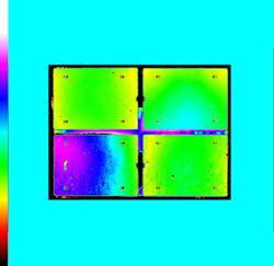
Figure 3 is the acoustic image showing four rafts. The gate from which echoes were collected for imaging extended from the interface between the metal heat sink and the solder to a depth partway into the raft. The round-trip transit time of echoes from the interface is being used to map the surface of this interface.
Three of the rafts are mildly warped, as seen by the yellow color of the corners. But the raft in the lower left is seriously warped, as shown by the much broader color range. There also are a few small voids in the solder, visible as acoustic shadows because they locally block echoes from the interface. The four regularly placed features in each image are posts.
Matched acoustic micro-imaging systems can inspect for this anomaly by collecting echoes from a narrow (i.e., vertically thin) gate that includes the surface of the solder layer and of the adjacent ceramic raft. If the surfaces are both level and well bonded, the resulting acoustic image will be of the same uniform shade of gray throughout.
But if the raft is warped, the image will have two or more regions depicting the varying depths of material interfaces. There will be boundaries, probably somewhat indistinct, separating these regions.
Applying the matched tool concept gives manufacturers the assurance that IGBT modules, or other items, being produced at various locations are structurally identical in their internal details. If anomalies appear in one production line but not in others, supervisors can know—because the acoustic micro-imaging systems are matched—that the anomalies are restricted to that one line.
About the author
Tom Adams is a freelance writer and photographer who has written more than 500 articles for semiconductor and microelectronics trade magazines.


