Stepping up to a vector network analyzer for IoT design optimization
With the acceleration of Internet of Things (IoT) devices and the proliferation of RF and wireless products, there is a growing need for RF measurement expertise and affordable RF test instrumentation. Until recently, vector network analyzers (VNAs) have been too expensive and hard to use for IoT and other embedded applications where they can be quite useful for design verification and optimization. That is now changing with the introduction of affordable, compact USB-based VNAs. Here, we’ll walk through VNA operation, discuss how they compare to spectrum analyzers, outline several key application areas, and look at how the emergence of IoT applications is changing RF instrumentation.
VNA operation
The VNA was invented in the early 1950s and was defined as an instrument that measures the network parameters of electrical networks. VNAs have gone on to make countless modern wireless technologies possible and are used in a wide range of RF and high-frequency applications. In design applications, simulations are used to accelerate time-to-market by reducing physical prototype iterations. VNAs often are used to validate and optimize these design simulations. In manufacturing applications, RF components or devices are assembled and tested with VNAs to ensure they meet specifications.
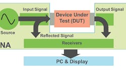
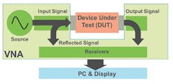
A key feature of a VNA is that it contains both a source, used to generate a known stimulus signal, and a set of receivers, used to determine changes to this stimulus caused by the device-under-test (DUT). Figure 1 highlights the operation of a VNA. For the sake of simplicity, it shows the source coming from Port 1, but most VNAs today are multipath instruments and can provide the stimulus signal to either port.
The stimulus signal is injected into the DUT, and the VNA measures both the signal that’s reflected from the input side as well as the signal that passes through to the output side of the DUT. The VNA receivers measure the resulting signals and compare them to the known stimulus signal. The measured results are then processed by either an internal or external PC and displayed.
A variety of VNAs on the market offers different numbers of ports and paths. In the case of a one-port VNA, the DUT is connected to the input side of Figure 1 and only the reflected signals can be measured. For a two-port, one-path VNA, both the reflected and transmitted signal can be measured; however, the DUT must be physically reversed to measure the reverse parameters. For a two-port, two-path VNA, the DUT can be connected to either port in either direction because the instrument can reverse the signal flow so that the reflections at both ports, as well as the forward and reverse transmissions, can be measured.
Understanding VNA specs
When comparing VNAs and matching an instrument to an application, it’s important to pay close attention to these four top-level specs: frequency range, dynamic range, trace noise, and measurement speed.
Frequency range is the first and most critical specification to consider. While all DUTs have an operational frequency range, you may need to consider harmonic frequencies as well. Active components—such as amplifiers, converters, and mixers—may need to be tested at their harmonic frequencies which are two to five times operational frequency. Filters and duplexers also may need to be tested at harmonics of their passband. Although a higher frequency range may be desired, maximum frequency range can be a major cost driver for VNAs.
Dynamic range is the measurable attenuation range from max to min over a specified frequency range. Based on the desired performance of your DUT, ensure that the magnitude of your maximum DUT attenuation specifications are at least 3 to 6 dB less than the VNA dynamic range specification. Most VNAs today offer very good dynamic range (up to 120 dB), which is sufficient for most common applications.
Trace noise measures how much random noise is generated by the VNA and passed into the measurement. It typically is measured in milli-dB (0.001 dB). Trace noise can be a key factor in determining the accuracy of certain components. An example may be the acceptable level of ripple in the passband of a filter. If you need a certain level of performance to determine accuracy of a signal through a filter, the added VNA trace noise contribution may be a factor.
Finally, one of the other specifications to consider is measurement speed: the time it takes to perform a single sweep or measurement. This can be a critical requirement for high-volume manufacturing applications. If you consider a component that is used in a smartphone, there may be billions of components made each year, and reducing test times at very high volumes is critical. However, for many design and low-volume production applications, the VNA measurement speed is not an issue.
VNA vs. spectrum analyzer
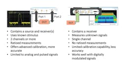
Many IoT design engineers have prior experience with oscilloscopes and spectrum analyzers but are less familiar with VNAs. But what’s the difference between a network analyzer and a spectrum analyzer? When would you need one or both instruments? Figure 2 provides a comparison of each instrument.
Spectrum analyzers are the instrument of choice when measuring digitally modulated RF signals. If the goal is to measure, for example, the performance of Wi-Fi and LTE signals, only a spectrum analyzer can perform these measurements.
Spectrum analyzers often are used to measure unknown signals, which may be over the air via an antenna or the output of a component. On the other hand, VNAs do not measure signals generated by a DUT. They measure the inherent electrical characteristics of devices themselves.
With a known stimulus and multiple receivers, the VNA can accurately measure the complex impedance and transmission characteristics of a DUT. This vector information is what allows for complete device characterization. Greater accuracy and dynamic range also can be achieved using vector error correction. This unique user calibration capability allows VNAs to factor out the influence of cables, adaptors, and fixtures.
Some spectrum analyzers offer built-in tracking generators, which give them some of the same capabilities of a VNA. The key difference between the two instruments is the VNA’s capability to measure signal ratios using multiple receivers. The spectrum analyzer with a tracking generator can make one-port reflection measurements and two-port transmission measurements. However, spectrum analyzers only perform scalar network measurements because they don’t provide phase information or perform error correction with phase, which results in lower accuracy.
User calibration
Among RF and microwave test equipment, VNAs have unique calibration techniques. While VNAs are similar to other RF and microwave test equipment in that they come factory calibrated and often require an annual check-up to be sure that they are still operating properly, VNAs have an additional “user calibration” that can be performed prior to making a measurement.
Having a known stimulus and receivers built within the same instrument gives the VNA the capability to achieve high-accuracy measurements. Since the VNA measures both magnitude and phase, the user calibration essentially performs a vector error correction. This is what makes the VNA one of the most accurate RF test instruments available. User calibration enables the VNA to factor out the effects of cables, adaptors, and most things used in the connection of the DUT. By removing the influence of the accessories, the user calibration allows for the exact measurement of the DUT performance alone. This enables designers to validate DUT performance when it is placed into a subsystem.
There are several types of VNA calibration physical standards used in the user calibration depending on the type of calibration method. The most common calibration standard set is referred to as Short, Open, Load, and Thru (SOLT). A VNA user calibration is performed using these known standards with a short circuit, open circuit, a precision load (usually 50 Ω), and a thru connection. It is best if the calibration standard has the same connector type and gender as the DUT. This allows for the DUT or calibration standard to be the only change between calibration and measurement.
Typical VNA measurements
VNAs perform two types of measurements—transmission and reflection. Transmission measurements pass the VNA’s stimulus signal through the DUT, which is then measured by the VNA receivers on the other side. The most common transmission S-parameter measurements are S21 and S12 (Sxx for more than two ports). Swept power measurements are a form of transmission measurement. Some other examples of transmission measurements include gain, insertion loss/ phase, electrical length/delay, and group delay. Comparatively, reflection measurements measure the part of the VNA stimulus signal that is incident upon the DUT but does not pass through it. Instead, the reflection measurement measures the signal that travels back toward the source due to reflections. The most common reflection S-parameter measurements are S11 and S22.
Swept frequency measurements
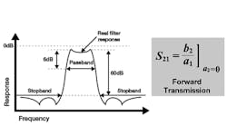
Swept frequency measurements are particularly useful. They sweep the internal source across a user-defined set of frequencies and step points. A wide variety of measurements can be made from this including S-parameters, individual incident and reflected waves (for example, a1, b2), magnitude, and phase. Figure 3 shows an example of a swept frequency transmission measurement of a passive filter. This type of filter measurement shows what happens to the signal as it passes through the component. The S21 measurement indicates the passband bandwidth performance as defined by its 6-dB response. The stopband performance is displayed as compared to a 60-dB reduction specification. The measured result then can be compared with the filter design goals or, from the system designer’s perspective, the filter manufacturer’s specification.
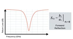
Swept frequency measurements also may measure reflections of the stimulus signal that are incident on the DUT, but are reflected as opposed to being transmitted through the DUT. These S11 (or Sxx) measurements allow the user to check and compare the performance of the DUT to its specifications.
Typical DUTs include antennas, filters, and duplexers. Figure 4 shows an example of an antenna return loss measurement. Note that in the antenna passband, most of the signal is being transmitted so a visible null occurs in the reflection measurement result.
Time-domain measurements
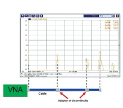
Some VNAs can use inverse Fourier transforms to convert swept-frequency measurements into the time domain. Data displayed in the time domain allows the VNA to be used to find problems in cables and connections by detecting the locations of impedance mismatches or discontinuities as the signal passes through the DUT.
For time-domain measurements, the capability to resolve two signals is inversely proportional to the measured frequency span: the wider the frequency span, the greater the capability of the VNA to distinguish between closely spaced discontinuities. The maximum frequency span is set by the user and may be defined by either the frequency range of the VNA or the viable bandwidth of the DUT.
Data collected in the frequency domain is not continuous, but a finite number of discrete frequency points. This causes the time-domain data to repeat after the inverse of the frequency sample interval, a phenomenon called aliasing.
It is important to set the frequency sample interval correctly to measure the required distance accurately to evaluate the DUT’s performance before aliasing occurs.
Figure 5 shows a VNA measurement of a cable with several adapters. This could be a base-station cable running from the base-station subsystem to its antenna. The time-domain measurement locates the physical distance to the different adapters or potential discontinuities in the cable, which helps locate problem areas or faults.
Swept power measurements
Instead of sweeping frequencies, VNAs also can sweep the stimulus signal’s output power level. For these measurements, the frequency is held constant while the output power is incrementally stepped across a defined power range. This is a common measurement for amplifiers, starting at a low power level and incrementing the power at fractional decibel steps.
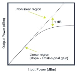
In the linear region of an amplifier, as the input power increases, the output power increases proportionately. The point when the amplifier output deviates from the linear expectation by 1 dB is referred to as the 1-dB compression point as shown in Figure 6. When the amplifier reaches its compression point, it is no longer able to increase its output power as before. For applications that require linear performance of an amplifier, this measurement helps define that specification.
Testing multiport components
Many components today have more than two ports. They may have one input and multiple outputs or vice versa. More complex components can have multiple inputs and multiple outputs. If the interaction between the ports is not a concern, some of these components may still be tested with a series of two-port measurements.
When there’s a need to measure the interaction between multiple ports, you may need a multiport VNA. A true multiport measurement would measure N2 S-parameters and require a VNA with N ports, where N equals the number of DUT ports. Instead of only S11, S21, S12, and S22, the S-parameters would also include S41 or S43, for example. The true multiport VNA can provide a stimulus signal to each of the ports. Multiport error correction removes systematic errors for the measurement but requires a complex calibration process where calibration standards must be connected to all possible combinations of ports.
VNAs meet IoT design
The growing adoption of IoT devices is driving a shift toward new workflows and lower cost instrumentation to meet shrinking time-to-market windows and to deal with increased project workload and decreased budgets. IoT designers tend to use precertified RF modules and often look to avoid RF testing when possible. In many cases, this is because RF experts tend to share expensive, high-end equipment across groups, a less than ideal situation when pressed for time.
This dynamic is starting to change with the introduction of USB-based VNAs and spectrum analyzers that are typically 40% or 50% less costly than traditional desktop instruments with equivalent performance. USB-based instruments eliminate the need for an integrated PC for signal processing. Instead, the instrument is operated via a user-supplied PC, laptop, or tablet running signal-analysis software. This allows test and measurement manufacturers to take advantage of the economies of scale and continual advances in the PC industry. As shown in Figure 7, this along with the IoT is driving a shift toward lower cost instruments.
Tektronix’s entry in the USB-based VNA market is a full two-port, two-path S-parameter VNA that features a 100-kHz to 6-GHz frequency range, 122-dB dynamic range, and -50- to +7-dBm output power in a compact package weighing less than 4 lb. Supporting software has a traditional look and feel for controlling and calibrating the instrument with a point-and-click interface. (Editor’s note: the article on page 28 describes the Tektronix VNA in more detail.)
Given the versatility and accuracy of VNAs along with the affordability of USB-based instrumentation, it may be time to consider adding a VNA to your IoT and RF design toolkit.
About the author
Dylan Stinson is an RF product manager at Tektronix in Portland, OR, where he manages RF/microwave instruments including the TTR500 Series vector network analyzers and RSA306B, RSA500, and RSA600 USB spectrum analyzers. He has a degree in computer and electrical engineering from Oregon State University.
