Designer adaptation in the changing PCB industry
The printed circuit board (PCB) industry, like almost all in the technology sector, has experienced extraordinary growth and change since its inception in the early 20th century. Changes in component packaging; increased demand for smaller, lower power devices; and ongoing advancements in the production methods of printed circuit boards have resulted in great advances in our everyday experience as users of electronic devices, along with far greater accessibility to technology and other services. One of the costs of such advancement is the need for those who design electronic devices and the PCBs they’re mounted on to constantly adapt to change, to learn new skills, to develop new ways of designing, and to embrace new tools along the way at a breakneck pace. Those unwilling or unable to make the necessary adaptations, as Darwin would put it, go the way of the dodo.
This article discusses the kinds of changes designers need to be willing to embrace in order to adapt—in mindset, in knowledge, in methods, and in tools. It does this by first examining the history of the PCB industry and waves of designers who fell by the wayside, giving up on a design career, versus those who made the necessary changes and adapted to survive and thrive in such a rapidly changing environment. We will look at the evolution from point-to-point soldering to PCBs with through holes, from tape-and-mylar to CAD, and from through-hole to surface-mount technology (SMT) and newer package types, and we will see what attributes surviving designers maintained through these transitions.
We then look to the future and speculate on what changes are coming, from current high-speed HDI to molded interconnect devices (MIDs) and similar examples, and on how both designers and their tools will need to adapt to take on the next evolutionary steps in this industry.
The PCB industry: a wild ride so far
Of all human endeavors, that of manipulating electrons for mankind’s use arguably has had the most rapid and amazing growth and change among industries.
You may think the Earth is at least about 10,000 years old, or at least a few billion. No matter what your scientific persuasion, when you consider that less than a single human lifespan ago, the first digital computers were developed and utilized the physics of thermionic electron flows through a vacuum, you must admit a lot has changed in a very short amount of time.
And as a foundation of the electronics industry, the technology of printed circuit boards—let’s just say printed circuits, as eventually there may be no board—has experienced equally profound changes. It’s little wonder that those who developed electronic devices over the past century have been jostled and shaken. Like the proverbial apples on a cart, many are left bruised and muddy on the side of the road as the cart hauls over rock and rut.
As electronics and PCB designers, we must be ready to learn, grow, and adapt. Keeping an open mind to the future, and possessing street smarts of lessons learned from the past, will help us survive and thrive in a volatile industry.
The early days
In the 1920s and 1930s, the first printed circuit boards were simple wafers of paper treated with phenolic resin. They had brass tabs and eyelets for soldering components onto, which in the 1940s evolved to the copper-foil laminated and etched PCBs still used to this day. The earliest of these were often used in “cordwood construction,” like the IBM 700 logic module,1 with axial resistors, diodes, and capacitors hand-soldered to the assembly. Needless to say, even though the new technology of computers was an enabler, components and manufacturing techniques had to evolve to add features, reduce power consumption, and reduce manufacturing costs and time.
Electronics were defined by electrical engineers drawing out schematic diagrams, standardized by IEEE and ANSI many decades before the invention of the PCB. Because of the hand-soldered point-to-point assembly techniques, electrical engineers would take a design straight from the test bench to work with mechanical drafters on wiring plans for the assembly line.
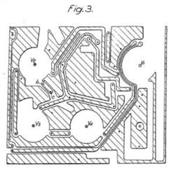
The earliest clearly documented PCB invention I can find is the original British patent issued to Dr. Paul Eisler, a Jewish Austrian who fled to the U.K. at the onset of World War II (Figure 1).2
Semiconductors
With the invention of the transistor, not only did the components and power supplies shrink, but the humble PCB was a natural choice for rapid assembly and reliable, repeatable quality as a substrate. But the new technology introduced new challenges.
Moving from a system where engineers would take their schematics from point-to-point factory wiring to the printed circuit created demand for dedicated interconnect designers. New jobs opened up in the industry and new drafting tools and techniques had to be created for PCB “artwork” to be developed and printed. Early designs were done using pen and ink directly on film.
Shrinking components with the invention of the bipolar transistor replacing electron tubes (or valves) meant having to work with far smaller geometries, while also moving to two-layer boards with plated through holes. PCB designers had to move to the photolithographic process where they could overlay multiple films with top and bottom copper layers designed with tape. Standard footprint stencils for common component types were made available by companies, such as Bishop, as self-adhesive decals or pressure-sensitive dry-transfers. These were still available for design and prototyping into the early 1990s. I remember buying them for my prototypes from the local Radio Shack!
With the shrinking components and board designs came both performance and assembly issues. On the performance side, designers had to develop—mostly through trial and error—an intuition for how wide traces ought to be for certain connections. With the introduction of ICs, standards bodies such as JEDEC worked with semiconductor manufacturers to standardize logic device “pinouts,” placing power and ground connections in consistent top-right and bottom-left fashions, making the layout of power and ground simpler. Designers established grid-based design practices to speed up the process, allowing them to lay tape on film in mostly orthogonal patterns with the concept of “layer bias” (for example, all horizontal traces on the top layer and vertical on the bottom). While practices like these evolved to help the efficiency of manual PCB design work, to a large extent they have stayed with us to this day. Digital PCB design was in its infancy, and circuits operated at speeds where engineers considered signal reflections to be a blessing that improved the quality of signals traversing the PCB.
Issues around design for assembly, design for test, and design for manufacturing all received attention during this time as well. The time-consuming and specialized nature of PCB design made it a necessary division of labor, with PCB designers now focused on assembly techniques and sequences while engineers focused purely on circuit design and analysis. Designers had to learn to keep suitable “courtyards” around component land patterns to allow factory workers and service technicians access to the parts for insertion and rework. Early boards did not always have solder masks. Trace spacings had to be broad enough to prevent solder bridging from the first generations of wave-flow soldering machines. This led, of course, to the idea of the solder mask. Designers had to create “pad master” films which enabled fabricators to create solder-mask screens for printing over the PCB surfaces. All along with the growth in the electronics industry, designers were “rolling with the punches” to adapt to new knowledge and techniques in the drafting process.
Moving to SMT, moving to ECAD
In 1981, EDA commercially began with an emphasis on semiconductor design tools. Graphical computing power at this time was only available to the government and large corporations. Most PCB layout was still done using mylar film and tape, but 1981 was also the year IBM introduced the PC—a move that would change everything.
In the early 1980s, miniaturization and manufacturing automation were the goal. JEDEC and IEEE sought to reduce PCB assembly size and production costs by coming up with SMT standards in which surface-mount devices (SMDs) could be machine-placed onto the PCB substrate. Designing with decals and tape on mylar was fine for the relatively bulky through-hole parts, but moving to surface-mounted resistors, caps, and ICs couldn’t easily happen without CAD, even though they were exclusive innovations.
The introduction of CAD tools for PCB design (aka ECAD or EDA) could be considered the first big inflection point that threatened the careers of PCB designers. Many PCB designers at the time, especially contractors, simply did not have the money to go out and acquire ECAD workstations. Some had the foresight to use capital to invest in the new ECAD systems to accelerate design and become highly competitive. If designers did not have budget for these Daisy or Apollo workstations (more than a year’s salary at the time) or lacked the time and capacity to learn to use software for design, they were forced into early retirement.
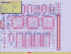
Fortunately, by 1984 the IBM PC and its clones became fast enough and had decent enough graphics displays that CAD became viable on the personal computer. As a result, some really nice, affordable, and approachable systems were released, including OrCAD (now Cadence) and Protel (now Altium). A late 1980s’ auto-routed reference design for SMT shows the traditional “layer bias” from the tape-and-mylar days (Figure 2). For a reasonable investment, PCB designers could get the efficiency of CAD. Of course, this meant a host of new issues to learn and overcome: CAD file transfer to manufacture, file formats, data storage and footprint, and symbol library management.
Source: Altium
Miniaturization: chip components to BGAs
The march of miniaturization continues. The 1990s brought significant density increases to semiconductors in the form of BGA devices.
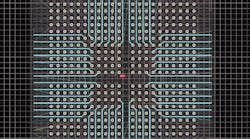
Now, PCB designers and their software tools had to become capable of “fanout” (Figure 3), the methods and patterns used to route the pads buried under the device to signals across the rest of the board. No longer could designs be restricted to two layers. Four- or six-layer PCBs became the mainstay, driven largely by the desktop PC and laptop markets.
Source: Altium Techdocs
War of the CADs
In the mid-1980s, there were many software companies starting in the desktop electronics design market. Designers had a big challenge in choosing the right tool that not only worked well for the types of designs they were doing, but as with all new software industries, knowing which vendor will be able to support you in the long run is largely unpredictable.
Designers have always faced and will continue to face a degree of uncertainty in this regard. Most of the foreseeable consolidation took place in the 1990s and early 2000s in the EDA industry; the main PCB design tool vendors took care of customers by providing migration paths for them.
We can’t deny this has caused pain for a number of designers over the years. Earlier CAD tools each had their own unique paradigms and mental models for circuits, components, physical board objects, layers, pad stacks, and modes of operation. Learning CAD software in the 1980s and 1990s invariably involved considerable time and mental energy, and moving from one CAD tool to another can be downright frustrating, especially for users who are experienced. As a support applications engineer, I’ve helped a number of people cross the line from PCAD to Altium Designer, and in the long run those who made the jump were very happy, but I would be lying if I told you there wasn’t collateral damage along the way. It’s inevitable. I remember one customer to this day, telling me they were considering getting out of PCB design as a career altogether simply because their main tool of choice was being discontinued.
But overall, those in the game consider the consolidation a good thing long-term (Figure 4); with more investment in fewer tools, those tools generally improve very much in usability and automation.
Speed kills
The continuous evolution of computing meant that by the mid-1990s, radio frequency, microwave, and high-speed (> 133 MHz) buses forced designers who previously just “joined the dots” to learn more about signal integrity (SI), length tuning, and impedance-controlled routing and layer-stack design.
Some PCB designers left the specification up to the engineers, which resulted in overly conservative, expensive boards with low yield. Others learned more about the qualities of PCB traces as signal transmission lines and actually applied pragmatic engineering to them.
Luminaries began championing the PCB designers who took the time to learn about RF, microwave, and high-speed signal propagation—people like Rick Hartley3 and Lee Ritchey4 who also taught PCB designers practical ways to design for high speed while maintaining reasonable specifications for geometries and layer stacks.
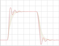
EDA companies making tools for PCB design jumped on the wagon by including simulation features (Figure 5) in their software for analyzing signal propagation and helped PCB designers and engineers determine reflection and crosstalk problems, along with driver and receiver compatibility issues.
Source: Altium Techdocs
Up to now
In the 2000s, it became apparent that PCB designers who may not have been electrical engineers had to adapt by developing at least a qualitative understanding of signal-integrity issues, helped along by Hartley, Ritchey, Eric Bogatin5 and others who are marvelous educators.
Collaboration outside PCB design used to be a matter of throwing a two-dimensional drawing over the wall to the mechanical engineer, and building cardboard mockups to check the form and fit of the PCB assembly with the final mechanical enclosure design.
As mechanical design cycles have embraced 3D printing for rapid prototyping, the means of collaboration have had to improve; we’re no longer designing multilayer 2D boards any more. Early attempts at transferring 3D spatial information about the board using IDF files just didn’t cut it. From 2006, ECAD was changed forever when the STEP file format was first introduced for components in Altium Designer 6. Other ECAD vendors followed suit.
The ongoing challenge of miniaturization and rapid development of the intelligent consumer device markets have made it imperative that, as designers, we continue to adapt. Although flexible circuits have been around for some time, flexible and rigid-flex-rigid designs are becoming more mainstream as the only means of reducing size.
Not only do designers need to learn about the fabrication and assembly issues and techniques for rigid-flex, even at the most basic level they need to be able to design them to form and fit right the first time—which is especially crucial when the costs of production are very high.
The road ahead: betting on the right horse
I guess my point is this: if you want to work in an industry where you get to be a lifelong learner, where you do cool stuff that forms the hidden magic in everyday devices, and you want to be on the cutting edge of technology, then PCB design is an excellent career choice.
But don’t be one of the apples that falls off the cart. Instead, bet on the right horse! This industry is constantly evolving, and with that evolution must come new tools and techniques—for example, 3D MIDs.6 These are intriguing, to say the least, with components and track work that can be any shape or angle around a molded plastic substrate.
Imagine 3D MIDs becoming multi-layer? It’s probably already happening. What we need are CAD tools for correct design and modeling, along with assembly equipment (pick and place, soldering, etc.) that can place the components at any angle. That’s just one example of where things are going. Flat rigid organic PCBs will certainly be with us for a while, but there’s always something new, too. It’s just a matter of betting on the right horse. And that horse could just as well be you.
About the author
Ben Jordan, senior product marketing manager at Altium, is a computer systems and PCB engineer with over 20 years of experience in embedded-system, FPGA, and PCB design. He started out at Altium as an applications engineer more than 13 years ago, traversing roles since as field applications engineer, tech support manager (USA), product marketing, and senior product manager. He is an avid tinkerer and is passionate about the creation of electronic devices of all kinds. Ben holds a Bachelor of Engineering (CompSysEng) with First Class Honors from the University of Southern Queensland.
References
- “IBM 700/7000 Series,” Wikipedia.
- “Manufacture of electric circuit components,” Patents, Google
- Warner, Judy, “PCB Designer Rick Hartley: Signal Integrity and High Speed Guru,” PCB Design Blog, Altium, June 27, 2017.
- Wyatt, Kenneth, “Review: Right The First Time, by Lee Ritchey,” EDN, Sept. 29, 2013.
- Bogatin, Eric, and Ramdurgkar, Ameya, “Analysis of a simple CTLE optimization algorithm for lossy channels,” Proceedings of the 2017 Electronic Design Innovation Conference, September 2017.
- “MID circuit carrier,” N&H Technology GmbH.
