Inspection, physical failure analysis complement electrical test
The areas of semiconductor test, inspection, and related technologies have seen considerable innovation during the second half of 2017. With regard to test, traditional ATE companies introducing new systems and instruments, while other test companies have been working on products ranging from components and instruments with semiconductor test applicability to systems and upgrade kits based on open modular architectures. Still other companies have been working on technologies ranging from reticle blank inspection to physical failure analysis.
SEMICON West, held in San Francisco in July, afforded semiconductor equipment makers one opportunity to highlight their latest offerings.1 The event opened amid good news, with Dave Anderson, SEMI Americas president, saying at a press conference, “The industry is doing great—2017 will be a record year.” In September SEMI was able to report that worldwide semiconductor manufacturing equipment billings for the second quarter were $14.1 billion—a record, representing an 8% increase over the first quarter of 2017 and a 35% increase over the same quarter a year ago.
At the show, many companies highlighted some of the equipment that contributed to the record global sales.
For example, Orbotech announced that imec has named its SPTS Technologies company as a new supplier of physical vapor deposition (PVD) solutions for under-bump metallization (UBM) and redistribution-layer processes for next-generation fan-out packaging technologies. Imec selected the SPTS Sigma fxP PVD solution for low-temperature PVD for development of novel fan-out technologies, such as flexible micro-bumps for chip scale packaging.
“To meet the technical requirements of future micro- and nano-electronics, novel 3D integrated-circuit architectures need to be developed to meet scaling challenges without compromising cost, performance, and power budgets,” said Kevin Crofton, president of SPTS Technologies and corporate vice president at Orbotech. “Imec works closely with leading semiconductor companies to develop innovative wafer-level packaging architectures that will meet the performance requirements of next generation devices such as application processors that drive virtual reality applications or enable high performance computing for artificial intelligence.” He cited in particular the SPTS Sigma for its 3D System Integration Program, reflecting the company’s PVD solutions’ results, particularly in low-temperature redistribution layer (RDL) and copper-pillar creation on low-temperature-tolerant polymers. “We look forward to working with imec and its partners in developing innovative interconnect and fan-out technologies,” he said.
For its part, UnitySC at SEMICON West marked its first year as an advanced process-control company developing, manufacturing, and marketing metrology and inspection solutions for heterogeneous integration. The company addresses advanced-packaging, sensor, and power-device applications using optical-based microscopy, interferometry, spectrometry, reflectometry, and other technologies. In the lead-up to the show, the company announced multiple orders from an IDM for its modular 4See Series automated defect inspection platform for power-semiconductor automotive applications.
In a recent article, Philippe Gastaldo, product and R&D director at UnitySC, highlights thin-wafer inspection challenges for volume manufacturing of power semiconductor devices related to backside polishing. He describes a technology known as phase-shift deflectometry (PSD) that measures the wafer-surface topography. “Companies that work with ultra-thin wafers are beginning to employ PSD technology that is both cost-effective and fast enough for high-volume manufacturing,” he writes.2
System-level test
Focusing on electrical test, Astronics highlighted its system-level test approach, aimed at smaller nodes that can result in missed transistors during traditional test and at advanced packaging techniques that can drive the cost of test escapes higher. The company highlighted its ATS 5034 system-level test platform, which can process up to 396 devices simultaneously.
The company notes that existing low-volume SLT equipment lends itself to the test of sample lots, which can lead to expensive test escapes. With its x396 massively parallel configuration, the ATS 5034 permits affordable 100% SLT. The platform can perform system characterization, system qualification, system-level test, and RMA/failure debug functions in applications including mobile devices, automotive computers, and biomedical-wearable and other IoT devices. The platform integrates the company’s ActiveATE software, which incorporates a test sequencer, devise manager, and integrated development environment.3
In addition, National Instruments and Marvin Test Solutions highlighted their PXI semiconductor test systems. NI displayed its Semiconductor Test System, or STS, with an emphasis on RF and wireless device test in conjunction with its vector signal transceiver (VST) technology. Marvin Test Solutions (MTS) exhibited its PXI Express-based TS‐960e, which MTS CEO Stephen T. Sargeant describes as the company’s highest end semiconductor test system.
Courtesy of Marvin Test Solutions
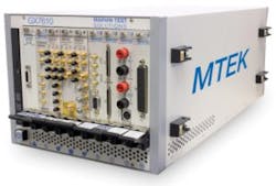
Several companies highlighted new products that will contribute to semiconductor equipment spending through the coming months and years. For example, MTS introduced the Marvin Test Expansion Kit (MTEK) Series (Figure 1), which offers a tester upgrade solution for legacy semiconductor test systems. “Those systems were designed and fielded years ago,” Sargeant said in a recent phone interview. “They may be running analog or digital or RF test, but many of those don’t have all three and may have only had one. So what we are able to do with the Marvin Test Expansion Kit is add the last one or the other two capabilities that they didn’t have before.” He added that over time MTEK can open the door to sales of the TS-960e, as customers learn about the company and its customer support through deployment of the METK systems.
Courtesy of Advantest
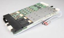
Advantest chose SEMICON West to highlight the addition of a mixed-signal channel card to its Wave Scale MX product family (Figure 2) for the V93000 platform. The new high-resolution, highly accurate mixed-signal channel card extends the Wave Scale MX product family’s range in testing analog-to-digital and digital-to-analog waveform converters, according to Hagen Goller, product manager for mixed-signal solutions at the company’s Böblingen, Germany, facility. The card provides high performance and fully independent AC and DC testing across as many as 32 instruments—16 arbitrary waveform generators and 16 digitizers—for either single-ended or differential signals. It has local, temperature-controlled references that ensure the highest DC stability over time, and single-ended signals can be referenced to a ground sense per channel to achieve high fidelity.
Advantest also launched the T5822 memory tester—the newest member of its T5800 product series. The T5822 is optimized for wafer-level testing of DRAMs, NAND devices, and other nonvolatile memories used throughout portable electronic devices, according to Jin Yokoyama, Advantest’s functional manager for the Memory/Storage Marketing and Business Development Department in Tokyo. The new tester offers high-voltage resources such a level driver and DC testing capability along with an economical compact test head. It also features a memory-repair analysis capability to help customers maximize their yields.
Courtesy of Pickering Electronics
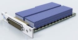
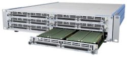
Pickering Electronics highlighted a new miniature reed relay with applicability to semiconductor test, according to Graham Dale, technical director at the company. The Pickering Series 120 comprises a range of single-pole reed relays that require a board area of 4 mm x 4 mm, he said. Figure 3 shows a total of 528 Series 120 reed relays on an ultrahigh-density PXI module. And since SEMICON West, sibling company Pickering Interfaces has introduced its Model 65-22x high-density modular LXI Ethernet matrices (Figure 4). A reed-relay matrix solution for semiconductor test and other applications combines Pickering’s LXI Modular Chassis (Model 65-200) with the new plug-in matrix modules that are constructed using Pickering Electronics’ reed relays. The companies plan to highlight their products at the International Test Conference October 31 through November 2 in Fort Worth, TX.
Courtesy of Pickering Interfaces
The range of modules includes four plug-in models covering matrices of up to 1,536 x 4 in increments of 128 (Model 65-221), 768 x 8 in increments of 64 (Model 65-223), 384 x 16 in increments of 32 (Model 65-225), and 192 x 32 in increments of 32 (Model 65-227). Users can specify as many (up to six) or as few plug-in modules as required and can field-upgrade the chassis to extend the matrix when necessary. Over 1,500 relays can be closed simultaneously for specific conditions for parametric testing.
Focusing on software, Optimal+ highlighted its efforts to get semiconductor makers and electronics manufacturers to communicate to determine the root causes of faults. The company was emphasizing what it is now calling SQN, or Suppliers Quality Network, which aims to break down barriers between component makers and OEMs in what company representatives called a “win, win” for everyone.4
Also new at the event was the Precis generator from Reno Sub-Systems, a producer of RF matching networks, RF power generators, and gas-flow management systems for semiconductor manufacturing. The new generator offers the highest-power solid-state microwave generator available for semiconductor plasma applications, the company said, adding that its approach to power generation fills a growing need for advanced subsystem technologies to keep the industry on pace with Moore’s law.
And although not exhibiting at SEMICON West, Xcerra’s LTX-Credence division took advantage of the show’s proximity to debut its DxV ATE system in a nearby venue. Xcerra executives described the system as offering “…full semiconductor ATE performance in a desktop PC footprint.” The DvX accepts up to five of Xcerra’s DiamondX DC to high-speed instruments, with more than 1,000 pin resources available for high-volume production needs. The DxV features a workstation fully integrated into the test head, making an external PC unnecessary.
Courtesy of LTX-Credence
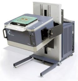
Xcerra has continued making news since the DxV’s debut. The LTX-Credence division announced in August that it has shipped the 600th PAx test system, with the latest system going to Skyworks Solutions Inc. The PAx platform (Figure 5) has been specifically designed to address the high-volume manufacturing test challenges of suppliers of advanced front-end RF devices such as multiband RF power amplifiers, RF front-end modules, RF and analog system-in-package (SiP) devices, and RF discrete devices. “Our goal with the PAx platform was to offer semiconductor manufacturers of RF front-end devices an alternative to deploying their own in-house test systems,” said Steve Wigley, vice president of the semiconductor tester group of Xcerra. “Our approach was to leverage LTX-Credence RF manufacturing test technology and use our systems expertise to package it in a compact footprint to offer the required levels of performance, fast test times, and operational availability.”
Handlers and contactors
Xcerra’s Multitest handler and contactor division has also made news, announcing that the Shanghai Industrial µTechnology Research Institute (SITRI) has added barometric-pressure-sensor test and calibration to its test-services offering. SITRI has extended its MEMS test capabilities based on an Xcerra Test Cell solution that includes an LTX-Credence Diamond tester, a Multitest InStrip handler, and the Multitest InBaro test module. “The Xcerra test cell approach combines the advantages of a completely pre-validated one-stop solution with the flexibility of a modular set-up,” said Gabriela Born, Xcerra director for InMEMS and IoT products.
Courtesy of Multitest
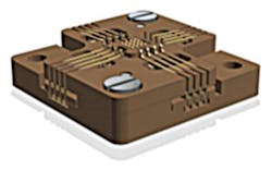
Multitest also recently announced that it has installed an MT9928 tri-temperature handler with an enhanced Soak Booster option, which cuts down the soak time by up to 50%. In addition, Multitest said that its new 0.3-mm-pitch Atlas contactor successfully passed a demanding customer production-floor evaluation. And finally, Multitest recently launched the MiCon contactor, which leverages cantilever technology for final test of microcontrollers, industrial DSPs, and application-specific ICs (Figure 6).
In related handler news, Boston Semi Equipment (BSE) announced that it has received an order for its high-voltage partial-discharge (HVPD) solution on the Zeus gravity test handling system. The order, for a quad-site handler, comes from a top 20 semiconductor company that selected BSE’s solution because, BSE said, the handler can position up to eight devices for testing and is designed for the high voltages the customer needs to test its packages. The HPVD solution using the Zeus system is capable of octal-site testing and integrates special materials and test-site design needed for effective and safe testing at very high voltages. In addition, the Zeus system’s device handling mechanisms have been optimized to ensure the effectiveness of high-voltage tests.
Electro-optical wafer-level test
Courtesy of SemiProbe
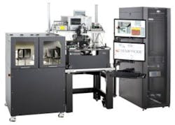
SemiProbe Inc. announced in July it has installed a 200-mm fully automatic electro-optical probe system (Figure 7) at VTT Technical Research Centre of Finland Ltd., which offers silicon photonics design and foundry capabilities. The organization will use the fully automatic probe system to perform automatic and simultaneous electro-optical tests at wafer level (E/O WLT) in support of VTT’s silicon-photonics (SiPh) volume production activities and offer advanced E/O test services to other users.
Dr. Timo Aalto, SiPh pioneer and team leader at VTT, commented, “In the past few years, SiPh has been one of the fastest growing areas at VTT. In 2016, we delivered thousands of SiPh chips for our customers, and, in 2018, the targeted volume of tested chips is over one million. E/O WLT is therefore vital in our R&D and manufacturing value chains.”5
SemiProbe built the system using its patented Probe System for Life (PS4L) architecture. Using PS4L technology, customers can reconfigure the system to add new modules and accessories as requirements change. These changes are made via field upgrades and are a fraction of the cost in comparison to purchasing a new system, the company said.
The system consists of four multi-axis programmable manipulators that provide automatic fiber-optic alignment and electrical contact. The entire system, including the prober, material handling unit, and manipulators, are remotely controlled through a customer-developed GUI using NI LabVIEW. The probe system will handle 150-mm and 200-mm wafers and can be operated in manual, semiautomatic, and automatic modes.
From reticle inspection to PFA
Many of the companies and products discussed thus far center on electrical test, but other news has dealt with topics ranging from reticle inspection to physical failure analysis. In the former category, KLA-Tencor has made news recently in the area of inspection of reticle blanks—composite substrates onto which reticle patterns are written. The company said although it has been a major presence in patterned reticle inspection since it introduced its first inspection system in 1978, its new FlashScan product line represents the company’s entry into the dedicated reticle-blank inspection market. The FlashScan systems can inspect reticle blanks designed for optical or extreme ultraviolet (EUV) lithography. The company said FlashScan systems leverage the laser scattering technology from KLA-Tencor’s wafer defect inspection portfolio and meet sensitivity and speed requirements for all optical and EUV blanks currently in production or development.
“Advanced lithography begins with a well-characterized reticle blank,” said Yalin Xiong, Ph.D., general manager of the Reticle and Broadband Plasma Wafer Inspection Division at KLA-Tencor. “Defect-free EUV blanks have been notoriously difficult to manufacture, driving up costs and delaying the benefits that EUV lithography may bring to next-generation chip manufacturing. Our new FlashScan blank inspectors capture a broad range of defect types on bare substrates, absorber films, and photoresist coatings. In addition, FlashScan systems feature higher throughput and sensitivity than other systems currently on the market, accelerating cycles of learning for blank manufacturers and mask shops.”6
Courtesy of Thermo Fisher Scientific
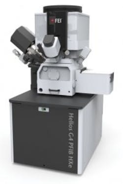
Addressing physical failure analysis, Thermo Fisher Scientific demonstrated three new additions to its portfolio of semiconductor failure-analysis workflows during the 24th International Symposium on the Physical and Failure Analysis of Integrated Circuits (IPFA 2017) in July in Chengdu, China. The new systems include the Helios G4 plasma focused-ion-beam (FIB) system (Figure 8), designed to deprocess and provide ultrahigh-resolution scanning-electron-microscope (SEM) analysis on a variety of semiconductor devices; the new flexProber system, used for fast electrical fault isolation to identify and locate faults both at the interconnect and the transistor levels of the semiconductor wafer; and the Themis S transmission electron microscope (TEM), designed to provide atomic-level resolution imaging and high-throughput chemical analysis on the most challenging semiconductor devices.
“The semiconductor market continues to evolve at a fast pace, with strong growth in the memory, foundry, Internet of Things (IoT), advanced packaging, and display markets,” said Rob Krueger, vice president and general manager, semiconductors, Thermo Fisher. “This growth has increased the need for fast, high-quality electrical and physical failure analysis. These products add new capabilities and increased flexibility to our existing portfolio of failure analysis solutions.”7
Advanced memory development
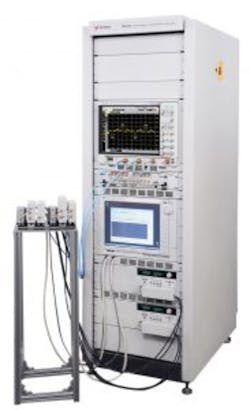
And finally, Keysight Technologies has recently turned its attention to accelerating the development of advanced memory—specifically spin transfer torque magnetoresistive random access memory (STT-MRAM), which is potentially the preferred next-generation nonvolatile memory. To characterize the magnetic tunnel junction (MTJ) component of ST-MRAM devices, Keysight in September introduced the NX5730A high-throughput 1-ns pulsed IV memory-test solution, which the company describes as a dedicated solution for researchers and engineers struggling with the characterization of MTJ devices on silicon wafers.
Courtesy of Keysight Technologies
The NX5730A (Figure 9) enables users to apply accurate and high-speed pulsed voltages (down to 1-ns pulse width) to switch the MTJ and to precisely and quickly measure the resistance of the MTJ before and after switching.
“Keysight’s new NX5730A stems from a collaboration with Tohoku University’s Center for Innovative Integrated Electronic Systems (CIES) STT-MRAM activities, which resulted in a successful outcome as announced in March of 2015,” said Masaki Yamamoto, general manager of Keysight’s Wafer Test Solutions.8 “Our customer experiences several challenges in MTJ characterization with conventional rack and stack-base test environments,” such as a time-consuming bit-error-rate tests, inaccurate writing voltage, and the difficulty of applying high-speed pulsed IV tests with 1-ns pulse widths. “The NX5730A is in direct response to our customers’ needs for MTJ characterization, and the NX5730A is already used in multiple memory research facilities, including CIES,” he said. “Moreover, Keysight continually develops its advance technology under CIES and Keysight collaboration.”
References
- Nelson, Rick, “SEMICON West addresses extended supply chain,” EE-Evaluation Engineering, September 2017, p. 26.
- Gastaldo, Philippe, “Overcoming thin-wafer inspection challenges for high-volume manufacturing,” EE-Evaluation Engineering Web Exclusive, Aug. 23, 2017.
- “ATS 5034 System-Level Test (SLT) Platform,” Astronics Test Systems Inc.
- Nelson, Rick, “OCMs, OEMs sharing data creates a win-win,” EE-Evaluation Engineering, October 2017, p. 32.
- “SemiProbe develops fully automatic electro-optical probe system,” EE-Evaluation Engineering Online, Aug. 13, 2017.
- “KLA-Tencor debuts FlashScan for inspection of optical and EUV reticle blanks,” EE-Evaluation Engineering Online, Aug. 16, 2017.
- “Thermo Fisher Scientific adds three products to semiconductor portfolio,” EE-Evaluation Engineering Online, June 29, 2017.
- “Keysight accelerates development of new memory, including STT-MRAM,” EE-Evaluation Engineering Online, Sept. 19, 2017.
For more information:

