Key trends driving the need for more semiconductor system-level testing
Decades of advances in the semiconductor industry continue to drive an insatiable consumer demand for smaller, more powerful, more ubiquitous semiconductor devices—whether in our cars, within our smartphones, or around our wrists. Likewise, testing methodologies must evolve to address this emerging complexity and comprehensively evaluate devices under test (DUTs) for defects that appear in real-world conditions.
While system-level testing (SLT) is not a new test methodology, it is a methodology that is gaining more attention, particularly for production testing. This is not only driven due to increased pressure to lower the overall cost of test (CoT), but also due to a number of technical drivers driven by lower technology nodes (which drive higher transistor count) and the increased complexity of devices.
This article covers some of those key trends and also points to the need for a massively parallel production SLT solution to best meet the need for testing today’s complex semiconductor devices.
The role of component-level system-level test
Historically for semiconductor devices, functional test was performed on traditional automated test equipment (ATE) as the test vehicle of choice. One would generate patterns, apply those patterns to a DUT, and then compare results to an expected outcome to evaluate whether or not the device met intended at-speed specifications.
As Moore’s Law continued to drive a higher number of transistors at each new (lower) node, the complexity of the devices also increased, so the addition of structural test helped reach a higher level of fault coverage in production. Utilizing techniques such as design-for-test (DFT) and built-in-self test (BIST) methodologies also helped to screen for manufacturing defects by exercising more transistors.
Many used SLT during this time, but it focused on qualification and preproduction validation. SLT enabled a test or product engineer to create an environment to test a DUT
in a way that closely resembled the final product. The engineer placed the DUT into a temporary socket on an end-product application board and used the actual firmware, device drivers, and operating systems to test how that DUT would operate and interact with the final hardware and software. The objective was to ensure that after integration into the final product, the device would meet its performance goals.
Eventually, as some of the leading early adopters of lower technology nodes emerged, there was a drive to add SLT as a production test step. Subsequently, there was a renewed interest in more massively parallel systems that could make burn-in and SLT more affordable. Devices such as CPUs, servers, graphics, and application processors required higher levels of massively parallel test.
Today, SLT is no longer purely a vehicle to validate a DUT in early qualification stages, but a valuable tool to reach maximum test coverage. Cost of test escapes, quality metrics, and the increased complexity of hardware/software interactions in conjunction with the trends listed below drive an increased reliance on SLT in production.
Trend 1: Lower technology nodes drive a higher number of untested transistors
Moore’s Law doubles the number of transistors with each lower technology node, yet the “percent coverage” of static ATPG (typically 99.5%) and at-speed ATPG (typically 85%) remains constant. This can create situations where emerging lower nodes can drive the number of untested transistors to unacceptable levels.
As shown in the Table 1, for a 22-nm technology node, there are 2.5 billion transistors and from the typical percent coverage, this equates to 12.5 million untested transistors with
99.5% static ATPG and 375 million untested transistors at 85% at-speed ATPG. While these might be considered acceptable levels of coverage, this test strategy becomes risky as devices move to the 7-nm technology node leaving 100 million untested transistors at 99.5% static ATPG and 3 billion untested transistors at 85% at-speed ATPG. Here, as the likelihood of untested transistors increases, so does concern for a greater number of test escapes.
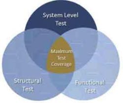
SLT provides an opportunity to increase the coverage for these untested transistors due to a methodology to test the DUT in its final product environment in production and, as needed, test critical paths in the device. In this way, SLT is complementary to structural and functional test because the mesh in the test strategy leads to maximum test coverage (Figure 1).
Trend 2: Concurrent scenarios are driving complex test scenarios
“Concurrent scenarios” refers to the reality of today’s leading-edge devices, where we require those devices to perform several activities simultaneously, creating situations where developing test patterns for every potential scenario is extremely difficult.
Consider this complexity with the example of testing a mobile device: you are in your kitchen using your timer while you are playing a game, downloading another application, and running Skype in the background. A phone call comes in and you want to ensure that the phone call gets priority while the other apps run in the background.
Another example highlighting a complex device-testing scenario might be for an automotive application: you are using navigation, playing satellite radio, pairing your phone to Bluetooth, and just as a call comes in, a car swerves into your lane. You need to be sure that the vehicle gives top priority to the swerving car over the other activities.
With traditional structural and functional test methodologies, generating, simulating, and debugging patterns to test these various scenarios can take months, and there is always a risk of yield overkill, or the throwing away of good parts that have registered a false positive. With SLT, however, generating and debugging for combinations of these types of scenarios can take minutes to develop.
Trend 3: Lower VDD creates higher concerns for guardband stack and yield overkill
As device geometries shrink with each generation of devices, so do the associated supply voltages (VDD). On the positive side, this helps to improve the battery life of a device, but on the other hand, it can have a negative impact on yield and result in “yield overkill.”
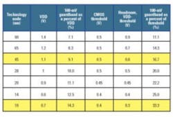
During functional test, the addition of a guardband stack (Figure 2) compensates for
worst-case system to ATE fmax/vmin deltas as well as ATE equipment variations. This guardband stack typically remains constant as devices move to lower node count and lower VDD. To pass a functional test, a device must be able to pass through the device headroom—which is the difference between the VDD supply voltage and the CMOS threshold (or turn-on voltage) of the device.
The result is that the guardband stack eats into this headroom, and the window for a “good” test shrinks as devices move to lower VDD and lower nodes. For example, at 45 nm, a 100-mV and 1.1-V VDD guardband consumes 16.7% of the headroom while at 10 nm and a 0.7-V VDD, the headroom consumes 33.3% (Table 2).
This conservative overkill can result in disposing of good parts that have registered a false positive through ATE testing. The use of SLT helps recover good devices that might have failed due to this issue. By providing test engineers with a tool to recoup these good devices that might have failed due to adding a guardband stack, SLT can also help to reject devices that would have failed in the final product.
Trend 4: DVFS explosion and PVT corners driving too many test scenarios
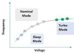
DVFS (dynamic voltage and frequency scaling) and PVT (process voltage and temperature) are two factors that design and test engineers must take into account in their testing today. Many new devices automatically change power modes to conserve battery life resulting in an increase in the number of modes and power conditions that require test. Ideally, testing should cover every possible power situation. For a device that has three modes—sleep, nominal, and turbo (Figure 3)—perhaps nine voltage domains per mode, and six power supplies for each domain, this can create a large number of patterns. DVFS explosion is the term we use to describe this phenomenon.
PVT refers to the variations in process voltage and temperature that, inherent in the fabrication of semiconductor wafers, also require simulation and testing. The “corners” in this context refer to the missed combinations and with the movement to lower nodes, the number of corners increases. For example, going from 65 nm to 16 nm could result in a 150% increase in the number of corners.
SLT can help in both of these scenarios. It has the ability to boot and run a device natively in different voltage modes similar to the end-user experience and run tests in each of those modes. For example, a device can boot in nominal mode, run multimedia in turbo mode, and sleep when not in use as part of a single, real-world test.
Trend 5: Conventional test methods no longer catch faults
New packaging technologies and increased device complexities also drive interest in SLT. 3D process geometries cause new defect types that traditional structural and functional test patterns do not cover. FinFET devices, for example, create new fault models such as fin cracks and via voids that can be difficult to test with traditional ATPG patterns. Another example is system in package (SiP) devices, where, even if each IP from different vendors provides 100% yield, combining differenet IP into a single package does not guarantee 100% coverage.
Due to their specific design, CPU and application processors can handle emerging applications that require substantially more compute power (for example, multicores for artificial intelligence). The embedded system must be able to handle faster I/Os to process
large amounts of data (for example, 4k video), which increases the potential for latency-related defects. Consumer devices must maintain or extend battery life, which requires greater power-management sophistication and the need to extensively test both boot and sleep/wake operations as described above. In addition, high-speed bidirectional interfaces such as PCI Express and USB 3.0 require faster read/write turnaround times that the inherent latency of ATE often cannot address natively.
In these scenarios, SLT can provide a method of additional fault coverage beyond what existing test coverage traditionally reaches and in a more cost-effective fashion—another advantage of a massively parallel SLT system.
Lowering the cost of SLT
As SLT becomes more important for production testing, the challenge becomes making SLT affordable. A lower cost of test (CoT) is a key enabler to adding more SLT to a test flow.
One challenge to overcome is that SLT test duration is often in minutes instead of seconds, proportionally driven by time required to boot, load the operating system, and shutdown for today’s embedded systems. Traditional SLT test systems, whether on ATE or low parallel SLT testers, offer diminishing returns at x16 parallelism. For minutes of test duration, the test platform requires hundreds of sites working in parallel for a similar CoT benefit at today’s ATE systems.
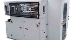
Implementing SLT in a massively parallel approach (Figure 4), with up to hundreds of DUTs tested simultaneously, has produced excellent results. These platforms are available today and help achieve a high unit per hour (UPH) throughput to keep escalating CoT in check.
SLT testers must also be able to test devices across a variety of applications to help reduce overall costs. For example, for automotive applications requiring hot/cold testing, SLT platforms today have the ability to add active thermal capability on a per-site basis; however, to be cost-effective, that thermal capability needs to reach targeted temperatures quickly.
Finally, the ability to support both low-volume/high-mix scenarios as well as scale up to massive parallelism can help customers leverage their investment across a wide portfolio of devices.
Conclusion
As we have seen, semiconductor testing historically focused on finding hardware defects on
a standalone device, but it is becoming more important to know that the device will work in its final hardware/software ecosystem. Production SLT can help manufacturers formulate test strategies that target emerging complex devices. This is especially important for consumer devices and in segments such as automotive and medical devices where lives depend on a product working flawlessly over time.
SLT helps to ensure optimal performance of the integrated “system,” gaining popularity due to a number of business and technical drivers discussed above. As the semiconductor test industry continues to evolve, we see increased production SLT emerging as a complementary testing methodology to structural and functional test as customers continue to find new ways to maximize test coverage for their emerging complex devices.
About the author
Anil Bhalla is a senior marketing manager at Astronics Test Systems and is a key contributor for the strategic planning of the company’s semiconductor test product line. Since joining Astronics in 2014, he has been active member of the SEMI System-Level Test (SLT) CAST and the SLT Heterogeneous Integration Roadmap (HIR) working groups. He has been a featured SLT presenter at SEMICON West’s Test Vision 2020, SEMICON Korea’s Test Forum, SEMICON China’s CSTIC, as well as a presenter on an SLT webinar hosted by EE-Evaluation Engineering. He has spent over 20 years in the semiconductor industry and previously worked at Verigy, Agilent, HP, and Advantest in a number of strategic positions. He holds a B.S. in Electrical Engineering from New Mexico State University and an M.B.A. from Colorado State University.


