Many engineers who use spectrum analyzers on a regular basis might be content to know that their instruments will produce a display of “power versus frequency” with little idea of what’s going on inside. Despite this, understanding the architecture of these instruments is important to maximizing their performance in practical applications.
An RF signal analyzer must downconvert signals from RF to a frequency range that can be digitized with an analog-to-digital converter (ADC) with anywhere from 12 to 16 bits of resolution. The mixer—and its frequency translation properties—is at the heart of the downconversion process, though I won’t focus on mixer theory of operation here (see “What’s Inside Your RF Signal Analyzer?”). Instead, I want to focus on two main vector signal analyzer (VSA) architectures, exploring both the theory of how they downconvert signals to baseband and the tradeoffs between them.
This file type includes high resolution graphics and schematics.
Single-Stage Downconversion
The single-stage downconverter is by far the simplest technique that can be employed to downconvert signals from RF to an intermediate frequency. The premise of this architecture is that a single broadband mixer (hence the term “single stage”) will be used to mix signals from a wide range of radio frequencies to a fixed intermediate-frequency (IF) filter.
Suppose a single-stage VSA uses a final IF frequency of 100 MHz that will be digitized by a 14-bit, 250-Msample/s ADC (Fig. 1). Given the choice of ADC, our example VSA will be sampling in the second Nyquist zone of our ADC, which would range from 75 MHz to 150 MHz. (The first Nyquist zone would be dc to 75 MHz.) Also, we’ll need a tunable local oscillator (LO) to drive the mixer, which is usually a voltage-controlled oscillator (VCO) in single-stage designs.
In practice, the single-stage VSA operates by tuning its LO to a frequency that is offset the signal of interest by exactly the IF frequency. Thus, to set a center frequency of 1 GHz on our VSA, the instrument must internally tune the LO to either 1 GHz – 100 MHz = 900 MHz, or 1 GHz + 100 MHz = 1.1 GHz. In the former case, setting an LO at 900 MHz is referred to as “low-side” injection, and setting the LO to 1.1 GHz is “high-side injection.”
Images In The Single-Stage VSA Design
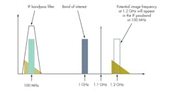
While our two frequency choices for an LO might seem beneficial, the notion of high-side and injection presents an inherent challenge in the single-stage architecture. Suppose we choose high-side injection in the example above, setting our LO frequency at 1.1 GHz. As it turns out, while we are “high-side injecting” the 1-GHz band, we are simultaneously “low-side injecting” the 1.2-GHz band.
Related Articles
• What’s Inside Your RF Signal Analyzer?
• Use Signal Analyzer To Measure Power Supply, Regulator & Reference Noise
• Signal Analyzers Cover Both Ends Of The (Cost) Spectrum
In fact, given that 1.2 GHz – 1.1 GHz = 100 MHz, and that 100 MHz is our IF frequency, any 1.2-GHz signal present at the RF port of the mixer will also pass through our IF filter and obscure the signal of interest. Figure 2 shows how signal content at the image frequency of 1.2 GHz will also mix to exactly 100 MHz in this scenario.
While this classic imaging scenario is common to all single-stage VSAs, the single-stage design is highly appropriate in a broad range of applications. Single-stage VSAs generally tend to have a smaller footprint and fast tuning times. They also typically cost less and still deliver excellent performance when analyzing modulated signals. As a result, the single-stage design is common where the frequency range of signals present at the RF port is reasonably constrained, such as production test of cellular handsets, wireless connectivity devices, and RFICs.
Image Rejection In The Superheterodyne RF Signal Analyzer
To deal with image rejection, many RF signal analyzers employ multiple mixing stages to adequately remove out-of-band signals from the band of interest. The three-stage design is relatively straightforward, though fully grasping how the frequency plan works requires a bit of mental gymnastics.
From the single-stage example, we learn that the “image frequency” is always exactly “one IF” away from the center frequency of the RF signal analyzer. Thus, if our VSA can filter signal content from the image frequency in the first place, then we can ensure that these images do not obscure the signal we are attempting to analyze. A classic solution is to use a first IF that is high enough in frequency so it will fall outside the frequency range of our instrument in conjunction with a low-pass filter.
Suppose we were building an RF signal analyzer designed to analyze signals from 20 Hz to 3.6 GHz. In this scenario, we could employ a low-pass filter as one of the first components in the VSA design to ensure that signals higher than 3.6 GHz are removed before ever hitting the first mixer. Next, we would choose a first IF that was sufficiently high in frequency to ensure that our 3.6-GHz low-pass filter has “cleaned” the image frequency.
Superheterodyne Frequency Plan Scenarios
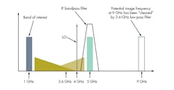
Given the requirements for a superheterodyne downconverter, consider a 20-Hz to 3.6-GHz VSA design where the first IF stage is at 5 GHz. High-side injecting a 1-GHz signal to produce an IF at 5 GHz would require us to set our LO at 4 GHz (1 GHz + 4 GHz = 5 GHz). Moreover, high-side injecting a 1-GHz band with an LO of 4 GHz means we are simultaneously low-side injecting the 4 GHz + 5 GHz = 9-GHz band. The 3.6-GHz low-pass filter already has “cleaned” this band, ensuring that images at this frequency do not obscure the band of interest (Fig. 3).
After the first IF filter of a superheterodyne signal analyzer, one can be reasonably sure that out-of-band signals have been removed by a combination of both the front-end low-pass filter and the IF bandpass filter. Next, subsequent mixing stages gradually mix the high-IF signal to second and eventually a third IF frequency—using band-pass filters to remove unwanted mixing products (Fig. 4).
In the three-stage design, multiple stages are used to ensure that at each mixing stage, the intermediate frequency at the output of each mixer is far enough from its mixing frequency to prevent imaging from occurring. Here, the rolloff of each of the IF filters primarily determines the likelihood of imaging, and using a second IF at a reasonably high frequency improves the instrument’s image rejection. In the end, the final IF is low enough in frequency to be digitized by the ADC. After digitization at IF, the VSA will digitally downconvert the IF signal to IQ and perform a complex fast Fourier transform (FFT) to present as spectrum information.
This file type includes high resolution graphics and schematics.
Parting Thoughts
The three-stage superheterodye vector signal analyzer uses a reasonably straightforward architecture to cleanly downconvert signals from RF to IF. Understanding these architectures will help you to understand how to optimize your VSA for making challenging measurements such as intermodulation distortion (IM3)—a topic we’ll save for next time!
David A. Hall is a senior product marketing manager at National Instruments, where he is responsible for RF and wireless test hardware and software products. His job functions include educating customers on RF test techniques, product management, and developing product demos. His areas of expertise include instrumentation architecture, digital signal processing, and test techniques for cellular and wireless connectivity devices. He holds a BS degree with honors in computer engineering from Penn State University.


