Point/Counterpoint: Today’s FPGA Prototyping—Breaking the Typecast Mold
Engineers often turn to two tools to verify their complex SoC designs: hardware emulation and FPGA prototyping. Some verification teams will use one over the other, while other teams remain confused about their differences and are looking for answers. Electronic Design called upon two experts to sort out the confusion. Below is S2C chairman and chief technology officer Mon-Ren Chene's case for FPGA prototyping. For the counterpoint case made for hardware emulation, see verification expert Dr. Lauro Rizzatti's "Hardware Emulation's Versatility."
We all know that complexities in design and shrinking time-to-market windows are driving up design and verification costs. Now more than ever, engineers are turning to hardware platforms to verify their designs on time.
FPGA prototyping platforms are growing in popularity due to their relatively low expense and ability to test system designs much faster than simulation. On top of being too slow, simulation often can’t provide an accurate assessment of design behavior.
Prototyping is often typecast as a solution used solely for small designs late in the verification process, just before the software development stage. The difficulties of employing this technology across multiple FPGAs have outweighed the cost and speed benefits of implementing large designs.
This file type includes high resolution graphics and schematics when applicable.
Emulation has been the choice for verifying large designs because of its capacity, but there are also limitations:
• It’s still slow for system testing, software development. and compatibility testing. Users require tens of replicates to do testing with the Internet of Things (IoT).
• Cost is high. Most companies can afford to implement a few emulators for early design verification. However, emulation costs soar when implementing for a large number of replicates for software development and compatibility testing.
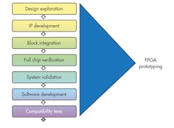
The truth is that today’s FPGA prototyping advances are breaking that restrictive, type-casted mold. Innovative hardware and the addition of cutting-edge software have made it possible to realize the benefits of FPGA prototyping, not only for system validation and software development, but also much earlier and throughout the design and verification flow. As a result, this technology is well suited for even the largest designs.
FPGA Prototyping Throughout the Flow
Utilizing a communication bridge that enables designers to read and write data from computers to their FPGA-mapped designs, engineers can easily implement algorithm validation, block-level prototyping, full-chip simulation acceleration, corner case testing and early SoC software development much earlier in the flow dramatically reducing the verification bottleneck (Fig. 1).
An example of this early communication and design exploration methodology is S2C’s ProtoBridge technology. ProtoBridge consists of a computer software component and an FPGA design component. The computer software component contains Linux/Windows drivers and a set of C-API/DPI routines to perform AXI transactions.
The FPGA design component contains PCI Express (PCIe), an interconnection module, and AXI transactors to be instantiated in users’ designs under test (DUTs). Users can read and write at speeds of up to 500 MB/s through the PCIe interface, connect eight master and eight slave devices on the AXI bus, and take advantage of the patent-pending Shared Memory technology that maps design memory space to computer memory for easy debugging.
A few use models include:
• C/C++: Users can develop tests in C/C++ and exercise the tests on an FPGA prototype at high speed.
• SystemC: Users can also develop design models in SystemC and link an OSCI-C simulator with FPGA prototypes through ProtoBridge.
• SystemVerilog: With DPI, users are able to take advantage of the verification environment developed in SystemVerilog to test their design in FPGA prototypes.
• Link with third-party ESL tools: S2C’s ProtoBridge, for example, has been integrated together with Mentor’s Vista and deployed in a number of verification flows. The integration allows the use of mature ESL models featuring advanced system simulation capabilities with part of a design in an FPGA-based prototype.
FPGA Prototyping for Big Designs
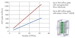
FPGA prototyping is well suited for even the largest designs. FPGA capacity has increased exponentially to 20 million ASIC gates per device, and up to half a billion gates in a single system is possible using an array of FPGAs. Next-generation FPGAs will likely double that capacity to one billion gates in a single FPGA system (Fig. 2). These capacity increases haven’t affected prototyping speed and costs, though, relative to emulation. Prototyping is still the much faster and cheaper option.
Yet, with these staggering increases in capacity, partition capability or compile time can be a concern. FPGA advances themselves have somewhat alleviated the partition challenge, since most IP/design blocks now fit into one FPGA, and partitioning designs at the IP boundary simplifies the task. Adoption of new FPGA I/O technology like 1-GHz LVDS enables delivery of more I/Os at higher performance between FPGAs using a pin-multiplexing scheme.
Finally, the quality and usability of partitioning software has improved substantially; as result, partitioning a design to tens of FPGAs has become more manageable. Although compile time is still longer than emulation, prototyping nonetheless offers a tenfold or more performance gain. Such benefits have made prototyping an irreplaceable technology, as it can be used for large software-development and -compatibility tests.
Debugging is a critical component during the verification of large designs. Advances in debug technology for FPGA prototyping have helped relieve concerns about debugging multi-FPGA partitioned designs.
In the past, debug tools only allowed visibility into the behavior of a design on a single FPGA, making debugging of multiple devices cumbersome and error-prone. In addition, these tools relied on the FPGA’s internal memory, reducing the amount of trace depth achieved and, in turn, only providing shallow visibility into design behavior.
Today’s debug technology erases these limitations by allowing for visibility of multiple FPGAs. At the same time, it eliminates crucial debug errors and dramatically reduces debug time. By using external memory, today’s solutions can also increase debug capacity to achieve deep design debug.
This file type includes high resolution graphics and schematics when applicable.
FPGA prototyping has always been the fastest and most cost-effective solution for verifying small designs late in the flow. Now, FPGA prototyping can be used throughout the process to find design bugs earlier, quickening the pace to software development. Increased capacity, scalability, and advanced partition and debug solutions have made FPGA prototyping the ideal solution for tackling today’s biggest designs.
Mon-Ren Chene, chairman and chief technology officer for S2C, has over 30 years of engineering and management experience in EDA and FPGA software/application development. He co-founded Osprey Design Systems that later merged with Aptix, where he served as software architect and VP of Software Development. Chene also held engineering and management positions at Quickturn Design Systems, Xilinx, Cadence Design Systems, Silvar-Lisco Design Systems, and NCA. He holds five U.S. patents and three pending patents. Chene graduated from Stanford University with an MS in operations research.


