Functional Testing and Validation for DDR4 and LPDDR4
Representing the most recent generation of double-data-rate (DDR) SDRAM memory, DDR4 and low-power LPDDR4 together provide improvements in speed, density, and power over DDR3. However, such speed and efficiency advances come at a cost. Not only do they require smarter memory controllers, new motherboards, DRAM, packaging, and software, but designers also must overcome the significant challenges presented by the shrinking timing margins at higher data rates.
JEDEC defines the specifications for protocol validation, but developers themselves are required to verify compliance. With no formal verification labs or test centers, individuals must decide on the appropriate procedures, methods, and equipment to perform functional compliance tests. To achieve the highest power savings, with the best reliability, designers and validation engineers will need to debug and validate the functional traffic flow for DDR4 and LPDDR4.
With each advance of DDR, higher clocking frequencies and data rates increase the impact of reflection and crosstalk on signal integrity, potentially causing signal degradation and logic issues. A shorter clock cycle also means a smaller jitter budget, while lower voltage swings make it more difficult to extract signals from noise.
Finally, perhaps the single greatest challenge for DDR4 and LPDDR4 design is probing. Because of the increase in data rate, the signal swing continues to decrease, causing the data-valid window (eye) to shrink. This makes obtaining a valid eye—without disturbing the system under test—extremely challenging.
Designers who first understand which of the new memory features to add to their system, and then overcome these timing challenges, will be the ones best positioned to meet customer needs.
This file type includes high resolution graphics and schematics when applicable.
DDR4 and LPDDR4 Features and Specs
DDR4 and low-power LPDDR4 enable significantly higher bandwidth for data transfer as well as improvements in speed, density and power over previous-generation memory. In addition to raw performance enhancements, there are over 20 new features added to DDR4 compared to DDR3, features that aid not only in performance but also in reducing power consumption, and improving manufacturability and reliability.
DDR4 is capable of up to 40% power savings over DDR3. LPDDR4 is targeting the highest data rates—at least 4266 million transfers per second (MT/s)—and burst lengths of 16 and 32 cycles (see the table). LPDDR4 presents significant changes in command implementation over LPDDR3, with multiplexed commands occurring over two or four clock cycles on the rising edge of clock only. The number of Command/Address (CA) bits has been reduced to six for LPDDR4, down from 10 for LPDDR3.
LPDDR4 on-die termination (ODT) settings are applied using Mode Register (MR) commands (instead of an actual ODT signal conserving an I/O pin). In LPDDR4, ODT can be applied to CA as well as the DQ bits. Depending on the ODT settings, LPDDR4 signaling voltage (at the balls of the DRAM) can be as small as 367 mV.
Comparing DDR Memories
| DDR3 | DDR4 | LPDDR3 | LPDDR4 | |
| Data rates (MT/s) | 2133 | 3200 | 2133 | 4266 |
| No. of banks | 8 | 16 | 8 |
8 and TBD |
| Burst Length | 4,8 | 4,8 | 8 | 16,32 |
| I/O Logic |
SSTL_15 stub series terminated logic |
Pseudo-open drain | HSUL_12 high-speed unterminated logic | LVSTL low-voltage swing terminated logic |
| Voltage (V) | 1.5 | 1.2 | 1.2 | 1.1 |
| Densities | 512 Mb - 8 Gb | 2 Gb - 16 Gb | 4 Gb - 32 Gb* | |
| ODT | Yes on DQ | Yes on DQ | Optional on DQ | Optional for CA and DQ |
*LPDDR4 reaches densities of up to 32 Gb with two-channel die.
LPDDR4 promises power savings over LPDDR3 that can exceed 40%. The greatest power savings occur during standby, since the low-voltage, swing-terminated logic (LVSTL) doesn’t draw current when not driven.
Functional Test Using a Logic Analyzer
Perhaps the best way to perceive signal timing is via functional testing with a logic analyzer. Following signal flow offers complete insight into the actual behavior of the memory system.
Accurate capture of data on a bus requires that the logic analyzer's setup/hold time fit within the data-valid window of the signal being sampled for accurate state-mode trace captures. Because the location of the data-valid window relative to the bus clock changes for different types of buses, the position of the logic analyzer's setup/hold window must be adjustable (relative to the sampling clock, and with fine resolution) within the data-valid window.
Today’s automated sampling-position tools hasten the tuning of the logic-analyzer sample positions for accurate state-mode trace captures. In addition, some logic analyzers allow users to view eye diagrams of the signals at the input to the logic analyzer.
DDR Eye Diagrams from Logic Analyzers
The eye diagram is a tool for deciphering high-speed digital buses. For DDR4, scanned eyes are smaller than eyes at the probe point due to logic-analyzer cable loss, jitter, and input bandwidth. Eyes scanned at the interposer are subject to reflections from the probing location on the bus, which isn’t the case with an oscilloscope’s optimized and de-embedded BGA probe.
These eyes are NOT used to qualify the DDR4 eyes at the DRAM, as they are when testing the physical layer. Rather, they can be used for qualitative comparisons and bus-level signal-integrity insight—the eyes compare signals scanned under the same conditions. Most importantly, they’re used to set accurate sample positions for logic-analyzer measurements.
Logic analyzers enable quick and confident validation and debugging of high-speed digital designs (up to 4 Gb/s). They offer the speed and features needed to see into DDR4 and LPDDR4 data-valid windows. Some logic analyzers have been optimized for protocol validation and debug specifically for DDR and LPDDR, including making reliable measurements on eye openings as small as 100 ps and 100 mV.
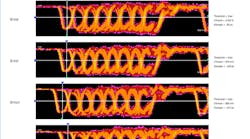
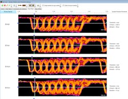
DDR eye-finder and eye-scan software tools help designers position the sampling points for accurate read and write data capture (Fig. 1). The software qualifies scans of valid read and write commands while the system executes memory tests, random read and write traffic, or stimulus programs. The software then displays read and write data-valid windows as a result of the scan. Users can compare hundreds of signals scanned relative to each under the same conditions for unparalleled qualitative insight into system behavior.
DDR eye scan makes it easy to determine the optimum acquisition sample point without requiring an oscilloscope. Scans can place the sample position at the center of the eye on every individual channel for maximum data-capture reliability, including separate sampling positions for read and write data.
DDR eye-scan technology in some logic analyzers provide insights that can’t be achieved with any other test method. It lets designers acquire signal-integrity information on all of a design’s buses, under a wide variety of operating conditions, in a matter of minutes. In turn, it problem signals can be quickly identified for further investigation with an oscilloscope. Results are viewable for each individual signal, or as a composite of multiple signals or buses.
In addition, DDR eye scan automatically groups signals so that designers are able to quickly spot byte-lane-related signal-integrity problems. Scans can be qualified based on state trigger criteria.
Signal Flow and Validating Functional Compliance
After inspecting individual DDR signals, designers will want to validate that the system is sending the correct DDR commands and memory banks are getting addressed properly, as well as check for protocol violations. A measurement tool is needed to separate read and write data signals, then display them at several levels of abstraction—from binary to protocol—to validate performance.
Multiple views and tools are available for functional debug and validation:
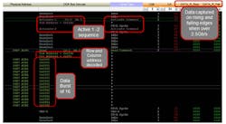
• The listing window displays decoder outputs (Fig. 2). Decoders take the raw trace capture and decode the signals according to the command truth table for the specific DDR/LPDDR bus. The decoder displays the row and column address information and DQ values associated with each read or write, making it easier for users to follow the flow of the memory bus traffic.
• State waveforms show the DRAM signals relative to each other as they were captured relative to the system clock. State traces can be up to 200-Msamples-deep per signal.
• High-sample-rate timing waveforms, which are up to 256-ksamples-deep, allow an oversampled view of when signals occurred relative to each other around the trigger point. Logic analyzer “timing zoom” captures can be adjusted around the trigger point depending on the user’s preference. Timing zoom traces are taken simultaneously with the state trace from the same probe point.
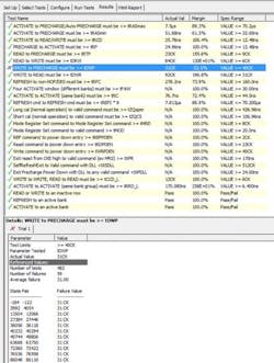
• Protocol compliance tools: The logic analyzer can trace for functional (protocol) violations to the JEDEC specifications (Fig. 3). Tools are automated to allow for repetitive captures.
• Real-time compliance tools set up triggers to capture traces of specific violations and to record pass/fail results. Tool automation runs through complete test suites.
Probing Effectively and Efficiently
Probing is the key to visualizing the best-possible signals. One solution—Soft Touch logic analyzer probes—can be used without connectors by just routing the traces in a specific manner. Their unique design makes solid contact with the traces. Flow-through routing can achieve data rates of 4 Gb/s. Placing the Soft Touch connectors close to the DRAM generally provides better eyes than mid-bus.
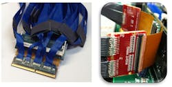
A DDR DIMM interposer is another solution, connecting directly to the industry’s standard DDR DIMM connector (Fig. 4). The non-intrusive design lets designers measure the full command, address, control, and data-bus signals.
For chip-down systems, the approach is to probe all DDR signals right at the BGA balls. One solution is to place a thin fixture between the DRAM and the board to access all DDR signals. For this, use DDR4 BGA probe interposers for JEDEC standard footprints. Figure 4 shows a side view of a DDR4 x4/x8 interposer installed under a DDR4 DRAM on a DDR4 dual in-line module (DIMM).
Choosing the Right Tool Vendor
New high-data-rate standards such as DDR4 and LPDDR4 create issues with optimizing performance, while meeting functional and parametric compliance to JEDEC standards. Designers intent on accelerating their mastery of next-generation testing and measuring protocols should strongly consider working with tool vendors that are active in JEDEC standard committee.
Close collaboration and communication offers designers access to the latest and greatest solutions for compliance testing. This is especially important for newly released technologies like DDR4 and LPDDR4, considering that the JEDEC standard committee is still in discussion about the specification and measurement. Although no formal plug fests exist for DDR, many tools are available to help you validate that your design is within compliance standards.
This file type includes high resolution graphics and schematics when applicable.
References
JEDEC Releases LPDDR4 Standard for Low Power Memory Devices, New standard to double memory throughput; Arlington, Va. ; August 25, 2014
JEDEC LPDDR4 Specification, JESD-209-4
JEDEC DDR4 Specification, JESD-79-4
