This file type includes high resolution graphics and schematics when applicable.
In 1973, Motorola employee Dr. Martin Cooper demonstrated the first ever mobile phone call—with a prototype that would eventually be released almost a decade later. A little more four decades after that moment in time, the total number of mobile connections in the world (now around 7.4 billion) exceeds the total number of people.
Looking into the future, ABI research recently predicted that by 2020, there will be more than 40 billion connected wireless devices—more than double today’s estimates of almost 20 billion (Fig. 1). From faster smartphones to smaller wearables to self-driving cars, these devices will use a broad range of wireless technologies, including LTE, Wi-Fi, NFC, Bluetooth, and ZigBee.
There’s little question that the explosion of wireless technology holds tremendous promise for consumer applications. However, the increasing volume and complexity of today’s wireless devices is fundamentally changing the cost dynamics of producing them. Wireless-device manufacturers are pressed with the challenge to dramatically reduce production costs and increase production capacity. However, at the same time, wireless devices themselves are becoming increasingly complex.
As a result, the need to lower test cost continues to drive significant innovation in the test and measurement industry. Not only has this market pressure driven the need for lower cost instruments, but it’s also driven a range of various new test techniques.
Increasing wireless adoption fundamentally changes the cost dynamics of producing wireless devices. Manufacturers are pressed to dramatically reduce production costs and increase capacity. However, the wireless devices themselves are only becoming more complex. As a result, the need to lower test cost continues to drive significant innovation in the test and measurement industry. Not only has this market pressure driven the need for lower-cost instruments, but it’s also driven a range of various new test techniques.
Greater Wireless Complexity
Higher device complexity increases test complexity and, without test innovation, results in higher test costs. Over the past 20 years, one of the most telling examples of increasing device complexity can be observed in the number of bands and cellular standards used in a mobile device.
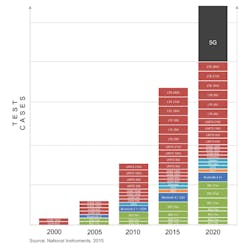
In 2000, it was common for a mobile phone to support two GSM bands. By 2005, mobile phones were using four GSM bands (marketed as “world band phones”) in addition to Bluetooth and Wi-Fi technology. By 2010, UMTS technology was beginning to augment the GSM/EDGE radio, and testing UMTS required completely new test cases. The trend of increasing wireless complexity has continued over the past five years with the rollout of LTE, 802.11n/ac, and even NFC (Fig. 2).
Looking forward to 2020, it appears that device complexity will only intensify. The industry may yet see widespread adoption of additional Wi-Fi technologies, such as 802.11p, 802.11ad, 802.11ah, and 802.11ax. In addition, the fifth generation of cellular communications will likely produce test challenges that far exceed that of LTE.
Current 5G research areas include the use of millimeter waves, new waveform types, new network topologies, and massive MIMO. Should millimeter waves or massive MIMO become adopted as part of the official 5G standard, mobile-device testing will get substantially more difficult and expensive.
More specifically, these wireless technologies will require test organizations to upgrade existing test infrastructure to support wider signal bandwidths, higher frequencies, and more antenna ports. Of course, these test requirements will pile on top of the new test cases coming from 5G.
Declining Cost of Wireless
Occurring simultaneously with the soaring complexity of wireless devices is the dropping cost expectations of wireless technology. In 1983, the first commercial mobile phone—the Motorola DynaTAC 8000x—retailed for $3995, which is almost $10,000 in today’s dollars. By 1990, a mobile phone cost less than $1000, and by 2000, a low-end mobile phone was priced at around $200.
Although the rate of decline in mobile-phone ASPs has slowed due to the increased value of smartphones, the price of the core wireless technology continues to drop. An excellent proxy for this was the 39% decline in ASP of Nokia phones from 2005 to 2009, a period over which smartphones represented a relatively low percentage of units shipped.
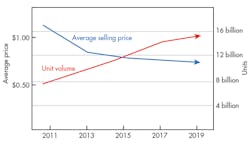
One of the most telling indicators of the “cost of wireless” can be observed by evaluating the ASP of the semiconductor components themselves. In fact, recent market forecasts by both Databeans Inc. and IC Insights predict that the ASP of mobile-device analog ICs will decline by more than 30% from 2011 to 2019 (Fig. 3).
Yet, the challenge of testing wireless devices requires a test approach that’s more extreme than a mere 30% improvement in test efficiency. In fact, coupled with the dramatic increase in device complexity, test efficiency must outpace both the challenges of test complexity and target test cost.
Factors such as increasing cellular bands, new waveform types, and more Wi-Fi configurations invariably lead to more test cases. Thus, the real challenge for today’s test engineers is not to validate the same number of test cases for 30% less, but to validate across 10X or 100X test cases for at least 30% less.
The Impact on Test
Although the idea of more-connected, less-expensive, and higher-throughput wireless devices is certainly appealing to us as consumers, it’s dramatically changing how wireless devices are tested.
A decade ago, mobile-phone testing required an instrument to literally place a cell-phone call with the mobile device. This approach, now called “signaling test,” requires a call to first be established before actual testing can take place. In some instances, phone calibration and testing can take 10 minutes or more.
More recently, the mobile-phone industry has shifted to the use of “non-signaling test.” With this approach, a PC can send a series of commands to the mobile device over a digital interface to get into a “test mode.” Although non-signaling test has proven to be a faster approach to device testing, engineers continue to innovate with faster test methods.
Today, both cellular and Wi-Fi chipset vendors are increasingly cooperating with test-equipment vendors to enable faster methods of wireless test. For example, new “fast sequencing modes” on modern wireless chipsets sequence through various test cases more quickly. This technique can be combined with faster instrumentation to test a wireless device faster and less expensively.
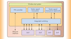
Going forward, the next major innovation in wireless test is the use of massively parallel or pipelined test architectures (Fig. 4). These test architectures reduce manufacturing costs by enabling manufacturers to test multiple devices in parallel to better utilize capital equipment. Today, an industry-wide shift is underway to replace 1-up (system test one device at a time) or 2-up test stations with more cost-effective 4-up and 8-up alternatives. Tomorrow, systems that test no fewer than 16 or 32 devices in parallel will no longer be cost-effective.
An Innovative Approach to Wireless Test
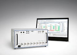
To address these challenges, NI has introduced the Wireless Test System (WTS), which packages the latest advances in PXI instrumentation with integrated switching and flexible software. This instrument is designed for high-volume manufacturing test of a wide variety of wireless technologies, from LTE Advanced to 802.11ac to Bluetooth Low Energy.
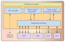
Internally, the WTS uses NI’s vector signal transceiver (VST), which combines a vector signal generator (VSG) and vector signal analyzer (VSA) into the same module (Fig. 5). In addition to the VST, the WTS also features integrated multi-port switching for parallel test or multi-port test applications (Fig. 6). With the integrated switching, engineers can configure the VST into a wide range of configurations, ranging from 8-up parallel test to parallel test of two 4x4 WLAN MIMO radios.
The WTS also features a unique software experience designed for high-volume manufacturing test. Although the WTS is internally a PXI system, engineers can automate it externally through SCPI commands over a remote Ethernet interface, allowing for easier integration into existing test infrastructure.
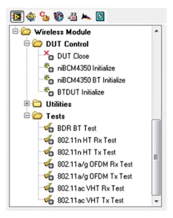
For engineers developing new test systems, the WTS user experience is aided by its integration into NI TestStand test executive software (Fig. 7). In fact, the TestStand Wireless Test Module features integrated command sets to control specific wireless chipsets and example code for typical tests.
Finally, the WTS is powered by high-performance multicore CPUs and FPGAs to accelerate measurement speed. Initial WTS customers were able to reduce test cost by combining WTS test speed with advanced parallel test techniques. As an example, peiker acustic’s head of test equipment recently stated, “WTS allowed us to reduce our test costs by more than 25%,” when testing multi-standard LTE/WLAN/GPS devices.
The Future
With increasing device complexity, wireless-device test will continue to require new approaches to test and measurement. As Frost & Sullivan Analyst Olga Shapiro recently stated, “To remain profitable in the future, companies will need to rethink their approach for wireless test and embrace new paradigms.”
Fortunately, the past decade has seen dramatic improvements in key instrument technologies, such as CPUs, FPGAs, VCOs, DACs, and ADCs. These improvements not only allow modern test equipment to deliver increasingly better analog performance, but also deliver increasingly faster measurement speed.
As one might expect, part of the solution for tomorrow’s wireless test challenges is a combination of lightning-fast instrumentation, a new approach to wireless test, and the engineering expertise required to put it all together. Fortunately, the need for test innovation is driving new solutions, and NI is empowering engineers to stop worrying about test—and get back to enjoying the soon-to-be 40 billion connected wireless devices.
