Download this article in .PDF format
A signal generator, a general-purpose piece of test equipment, performs numerous measurements for a variety of applications requiring electromagnetic wave signals as stimuli. Its roots trace back to the beginnings of the electronic test-and-measurement industry. The first product, developed by Hewlett-Packard Company (now known as Agilent Technologies), was the model 200A audio oscillator. One of HP’s first customers was the Walt Disney Company—in 1940, Walt Disney purchased eight audio oscillators to calibrate the breakthrough sound system it developed for the movie “Fantasia.”
Today, RF signal generators are widely used throughout the electronics industry, including aerospace/defense electronics and wireless communications. Typical applications include RF/IF signal generation and LO substitution, as well as radar, GPS, and avionics signal simulation.In modern wireless communications systems, signal generators supporting a range of digital-modulation formats are commonly used to test digital receivers and transmitters against increasingly complex requirements.
Regardless of the industry or application, getting the most value out of the signal generator requires a good understanding of its basic operation and function, as well as its key specifications. Another critical factor is becoming familiar with a signal generator’s ability to go beyond general-purpose applications to simulating advanced signals with impairments, interference, and waveform correction.
Table of Contents
2. Signal-Generator Architectures
- CW Signal Generator
- Analog Signal Generator
- Vector Signal Generator
3. Signal Simulation Solutions
The most basic signal created from a signal generator is the continuous wave (CW) signal, or sine wave, which has no modulation and is produced by a basic signal source. CW signals less than 6 GHz are commonly referred to as RF signals, while those between 6 GHz and 30 GHz and those greater than 30 GHz are called microwave signals and millimeter signals, respectively.
Many signal generators also offer various types of modulation, including analog and composite (digital) modulation. Classic analog-modulation types include amplitude-modulation (AM), frequency-modulation (FM), phase-modulation (ΦM), and pulse-modulation signals. Modulation is important because it’s the information-carrying part of the signal.
To better understand analog modulation, consider the basic equation of a sine wave:
In this equation, three parameters can be varied: amplitude, frequency and phase. Varying the sine wave’s amplitude achieves AM and pulse modulation. Varying the sine wave’s frequency or phase generates FM and ΦM, respectively.
Composite modulation, also known as vector or digital modulation, occurs when two or more modulation types are used to create a composite modulated signal. For example, AM and ΦM can be combined to create various magnitude and phase values. Varying the signal’s phase in conjunction with the AM control in the ALC circuit can produce a digitally modulated signal. It’s also possible to generate a variety of communications, satellite, and radar signals by employing a combination of pulse and either ΦM or FM.
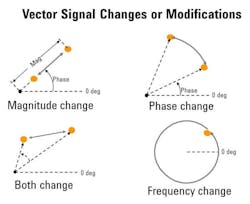
All types of modulation can be represented on a polar plane using vector (phasor) notation, although magnitude and phase values aren’t typically used when describing the vectors in digital modulation (Fig. 1). Instead, the polar plane is mapped to a rectangular format (with a horizontal and vertical axis) called the I-Q plane, where I stands for in-phase and Q denotes quadrature.
1. A magnitude change with no rotation represents amplitude modulation (AM), and a vector that rotates along an arc (the length of which indicates the maximum phase deviation) represents phase modulation (ΦM). Simultaneous AM and ΦM are indicated by a vector whose length and phase change with time. FM results in a vector that rotates clockwise or counterclockwise.
I/Q diagrams are particularly useful because they mirror the way an I/Q modulator creates most digital communications signals. Independent dc voltages (I and Q components) provided to the input of an I/Q modulator correlate to a composite signal with a specific amplitude and phase at the modulator output. Conversely, a modulated signal’s amplitude and phase sent to an I/Q demodulator correspond to discrete dc values at the demodulator’s output.
Quickly transmitting large amounts of binary bits at high rates in composite signals requires large information bandwidths. The faster the data rate, the wider the bandwidth. Available bandwidth can be used more efficiently by grouping blocks of digital data (1s, 0s) into symbols, although this increases signal complexity. The number of bits per symbol will vary depending on the specific format. Transmitting digital data via multi-bit symbols requires less bandwidth. For example, for two bits/symbol, the symbol rate is one-half the bit rate, and for four bits/symbol, the symbol rate is one-quarter the bit rate.
IQ or vector modulation, commonly used in modern digital communications and radar systems due to the large modulation bandwidths and ease in creating composite modulated signals, have a number of important characteristics. These include symbol rate (the number of symbols/second), modulation bandwidth (the maximum effective bandwidth of the IQ modulator), frequency response/flatness, IQ quadrature skew (a measure of how orthogonal the I and Q planes are to each other), and IQ gain balance (a measure of how closely the I channel and Q channel are in gain).
When the IQ characteristics aren’t ideal, magnitude and phase errors will occur that may cause transmission of incorrect digital information. Digital errors are referred to as bit errors, often expressed as a bit-error rate.
Signal-Generator Architectures
Signal generators come in different flavors: CW, analog, and vector. Each has a different function, and thus will find homes in different applications.
CW Signal Generator
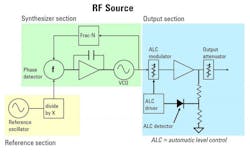
Looking at a basic block diagram of theCW signal generator, the RF CW source splits into three sections: reference, synthesizer, and output (Fig. 2). Thereference section supplies a sine wave with a known frequency to the phase-locked loop (PLL) in the synthesizer section. Its reference oscillator determines the accuracy of the source’s output frequency. The synthesizer section produces a sine wave at the desired frequency and supplies a stable frequency to the output section. The output section determines the overall amplitude range and accuracy of the source.
2. This basic block diagram of an RF CW source shows different reference, synthesizer, and output sections.
Within the CW source, the reference oscillator, phase detector, and voltage-controlled oscillator (VCO) all contribute to phase noise. The broadband noise floor also contributes in this regard. However, since it stems from the source’s thermal noise, it doesn’t greatly limit performance in most applications. Noise performance can be optimized by carefully selecting the bandwidth of the PLL in the synthesizer section. This determines exactly when the VCO contribution to overall phase noise becomes suppressed.
Like the RF CW source, a microwave CW source consists of a reference section, synthesizer section, and output section. The microwave CW source may also feature a number of differences, though. For example, although the reference section only has one reference oscillator, it may supply two or more signals to the synthesizer section.
Another difference may be the choice of oscillators in the synthesizer section. While RF sources generally use VCOs, microwave signal generators typically employ an yttrium-iron-garnet (YIG) oscillator tuned with a magnetic field. A PLL ensures frequency stability. In addition, output frequency range can be extended via frequency dividers and multipliers.
When determining the appropriate source for an application, it’s critical to first understand source specifications. For CW sources, the specifications generally divide into three categories:
• Frequency: The main frequency specifications are range, resolution, and accuracy. Range specifies the range of output frequencies produced by the source. Resolution specifies the smallest frequency increment. Source accuracy is affected by the reference oscillator’s stability and the amount of time since the source’s last calibration.
• Amplitude: The main amplitude specifications are range, accuracy, resolution, switching speed, and reverse power protection. Range is determined by the source’s maximum output power and amount of built-in internal attenuation. Resolution indicates the smallest amplitude increment. Switching speed measures how fast the source changes from one amplitude level to another. Reverse power protection helps prevent transmitted signals from the device under test from damaging the source.
Amplitude specifications have a direct impact on the CW source’s sweeping capability (the ability to move the CW tone in frequency). Frequency sweeps include ramp sweep, step sweep, and arbitrary list sweep. For ramp sweep, the source’s accuracy, sweep time, and frequency resolution are usually specified. For step and list sweep, the accuracy, number of points and switching time are specified.
In a frequency sweep, the output power varies by no more than the flatness specification throughout the sweep. CW sources also can sweep power level. When sweeping power, the amplitude sweep range determines the possible range of output powers, while the slope range determines how quickly the source can sweep from one power to another.
• Spectral Purity: Specifications associated with spectral purity (e.g., phase noise, spurious, harmonics, and sub-harmonics) can sometimes be difficult to understand. The ideal CW output is a sine wave at a single frequency—however, no ideal CW source actually exists since all are made with non-ideal (e.g., real) components that introduce phase noise and unwanted distortion products.
Harmonics represent integer multiples of the CW output. Sources contain many nonlinear components to provide a broad range of frequencies and output powers. The nonlinear characteristics of an amplifier create second-, third-, and higher-order harmonics. Non-harmonic spurs come from a variety of sources (e.g., power supply) and are typically quite low (less than −65 dBc). Finally, multipliers are often used to extend a source’s frequency output, resulting in the presence of sub-harmonics.
A number of applications can take advantage of basic CW signals, including use [OK?] as a local oscillator (LO) during transmitter development, for intermodulation distortion (IMD) testing of receivers, and for in-channel and out-of-channel receiver testing. Nonlinear amplifier testing is another key application. Third-order-intercept (TOI), a common amplifier measurement, uses two CW sources combined at the input of an amplifier (DUT). The amplifier’s nonlinearities produce third-order mixing products.
The test system itself also may introduce sources of error. These can be reduced either through better isolation of the signal sources, or by suppressing the power that transfers from one source to the other with a circulator.
Sweeping CW generators are most often used in stimulus-response testing (finding the DUT’s swept response). Frequency sweeps determine the frequency response of devices. Power sweeps, typically performed on amplifiers, measure linearity and saturation levels. When measuring a device’s frequency response, the important specifications are frequency accuracy, output power (level), flatness, and speed. Frequency-response measurements are made on many types of devices, including amplifiers, filters, and mixers.
Analog Signal Generator
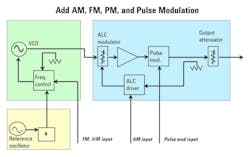
The block diagram of an analog signal generator is similar to that of a CW generator, except for additional components that allow the source to modulate the carrier (Fig. 3).
To create AM, the AM signal must be applied to the automatic-level-control (ALC) driver block, which converts voltages from the AM input into amplitude changes in the carrier through the ALC modulator. To create pulse modulation, a pulse input is added. That signal is applied to a pulse modulator in the signal’s output path. An internal modulator generator may be added to the CW source for convenience and to simplify test setups.
A key application for pulsed signals is radar testing. When creating a composite modulation signal like the chirped pulse, important signal-generator modulation specifications include FM deviation and rate, pulse rate, pulse width, and pulse rise time.
Vector Signal Generator
Creating a vector signal generator simply involves adding an IQ modulator to the basic CW block diagram. To generate baseband IQ signals, a baseband generator takes binary data containing the desired “information” to be transmitted, maps it to digital symbols and then to digital I and Q signals, converts the digital IQ signals to analog IQ signals, and sends them to the IQ modulator to be coded onto the carrier signal.
After the data undergoes symbol mapping, the digital signals are digitally filtered using two sets of filters in the baseband generator. The filters are designed to limit the bandwidth of the I and Q symbols and slow down the transitions between symbols. Many types of baseband filters exist, with each having different attributes that must be set in the signal generator. Common filter types are Root Raised Cosine, Gaussian, and Rectangular.
Vector signal generators are especially useful for simulating a wide variety of digitally modulated signals, including cellular, wireless LAN, Bluetooth, GNSS, and military communications formats. Some of the more commonplace vector measurements include adjacent channel power ratio (ACPR) and error vector magnitude (EVM).
ACPR is an important measurement, particularly for power amplifiers. It characterizes the distortion of digitally modulated signals and the likelihood that a givensignal may interfere with a neighboring radio. EVM and phase error are the two principal parameters for evaluating the quality of a digitally modulated signal. Measurement of these values entails examining the differences between a measured magnitude and phase vector of a digitally modulated signal and its corresponding ideal reference vector.
Another application revolves around measuring receiver sensitivity and selectivity. Sensitivity, one of the key specifications for a receiver, is the lowest possible signal level that can be reliably detected and demodulated. When making a sensitivity measurement, the signal generator’s level accuracy becomes an extremely important factor. Adjacent and alternate channel selectivity measures the receiver’s ability to process a desired signal, while rejecting a strong signal in an adjacent channel or alternate channel. Here, frequency and amplitude (level) accuracy, along with the spectral characteristics of the test and interfering signal, are important.
A vector signal generator can also be used in a Connected Solutions development environment. Connected Solutions is a concept that merges computer simulation with real-world measurements. Consider, for example, how desirable it would be to test receiver sensitivity before all of the receiver’s hardware blocks are available. Typically, bit-error-rate (BER) measurements can only be performed with the entire receiver. However, newer hardware and software development within test equipment now allows for BER measurements when just portions of the receiver are available. The Connected Solutions technique requires simulation software and test equipment to work together.
The process of simulating real signals includes waveform creation, baseband IQ signal generation, and upconversion of the IQ signals to the RF or microwave frequency of interest. While the vector signal generator and its associated baseband generator are core pieces to any signal simulation solution, other components may be necessary to simulate advanced signals.
For example, simulating fading impairments needs additional software and hardware to create the impairment and add it to the original signal. Luckily, modern vector signal generators can go beyond general-purpose applications to create advanced signals with various impairments and interference signals, providing a more realistic simulation of real-world environments.
While impaired signals are very useful for testing receivers under realistic conditions, other applications prefer a very clean, undistorted test signal. For example, the performance of an RF component could be evaluated by comparing its output to the input signal. In this case, a clean input signal ensures that the measured output reflects the device’s performance and not the input signal.
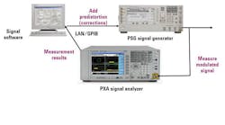
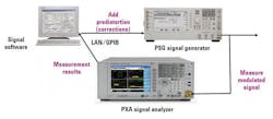
A signal generator has many potential sources of error (e.g., I/Q modulator, RF chain, and IQ path). Each of these affects the modulated test signal, resulting in an array of issues, including passband tilt, ripple, and roll off. Waveform correction provides a means of removing test signal imperfections (Fig. 4).
4. Waveform correction is accomplished by measuring the modulated vector signal generator’s output with a vector spectrum analyzer. Then those results are reported to signal correction software, which in turn predistorts the IQ data before it gets to the IQ modulator and effectively removes the imperfection.
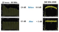
One type of vector signal generator imperfection is the amplitude flatness of the IQ modulator, or IQ flatness. IQ flatness can be viewed by creating 32 equal magnitude test tones within an 80-MHz bandwidth (Fig. 5). Notice that before waveform correction is measured and applied, the tones vary as much as 2.4 dB across the 80 MHz of interest. By measuring the vector signal generator in this mode and applying the appropriate waveform correction, tone amplitude variation reduces to less than 0.1 dB.
5. Waveform correction offers a means of addressing IQ flatness, although the tradeoff is calculation time and valid calibration time. Itis typically used on wideband, multitone, and multicarrier signals.
The same IQ correction can be applied to extremely wide band signals, such as the 500-MHz UWB signal shown in Figure 5. While it may not be possible to achieve 0.1-dB flatness on this type of signal, the performance nevertheless improves significantly.
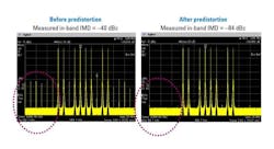
Another test signal imperfection concerns in-band IMD—the intermodulation products that fall within the channel bandwidth of the generated signal. Such distortion is particularly undesirable because it can’t be filtered and directly interferes with the signal-of-interest. This predistortion technique generates a canceling tone at the IMD frequency that’s 180° out of phase with the distortion product.
A spectrum analyzer is used to measure the IMD of the original test stimulus. Then, a predistorted waveform created from these measurements removes the in-band, as well as the out-of-band, IMD products (Fig. 6). By employing waveform correction, the vector signal generator provides much higher fidelity waveforms with a significant reduction in imperfections.
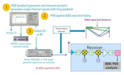
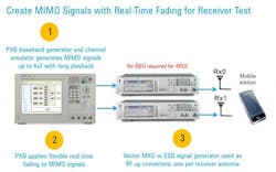
Other types of impairments, such as multipath signals or fading, can be simulated with appropriate equipment, such as the Agilent PXB baseband generator and channel emulator used in conjunction with the N5182B MXG signal and then added to the clean modulated signal in the vector signal generator. Examples include performance of single-input, single-output (SISO) test configurations and multiple-input, multiple-output (MIMO) receiver tests at RF/baseband (Fig. 7).
7. Multipath and fading impairments can be conquered with the appropriate hardware and software, as illustrated with these example SISO signal and fading tests (a) and MIMO receiver and fading tests (b) .
More information on Agilent’s signal generators can be found at www.agilent.com/find/sg.
