Verification via VNAs: Measuring PAM4 S-Parameters
Download this article in PDF format.
As high-speed serial data rates advance beyond 50 Gb/s, conventional logic-emulating non-return-to-zero (NRZ) signaling is being replaced by PAM4, a four-level pulse amplitude-modulation scheme. PAM4 takes half the bandwidth to transmit the same payload as the equivalent NRZ signal.
PAM4 challenges signal integrity, test, and design engineers who are responsible for SERDES components, interconnect, backplanes, cables, connectors, circuits, and complete systems. Why? Though PAM4 solves many issues associated with high-speed, high-bandwidth designs, its increased complexity means that a host of new issues must be addressed.
One critical condition is that PAM4 requires more accurate measurements. Designs must be verified before they’re produced—simulations and measurements have to agree on a point-by-point basis. Since signal-to-noise ratio (SNR) is about 10 dB worse for PAM4 than NRZ, qualitative agreement is no longer good enough. Simulation accuracy and channel evaluation begin and end with accurate measurements of S-parameters. For this reason, engineers must rely on a vector network analyzer (VNA) with specific performance benchmarks.
NRZ, PAM4 Bandwidth Demands
The limits of NRZ signaling were first approached in 100 GbE with its 25- to 28-Gb/s signals on four channels that combine to 100-Gb/s data payloads. Since each bit period covers half a cycle, the fundamental frequency of a 26.6-Gb/s NRZ signal is 13.3 GHz.
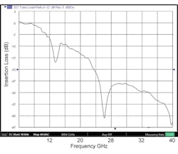
1. Insertion loss of conventional copper traces on a standard FR-4 PCB typically falls at about 10 dB per frequency decade. The effects of connectors, vias, BGAs, and other impedance mismatches in a real circuit will cause resonant peaks and absorption valleys.
The insertion loss of conventional copper traces on standard FR-4 PCB typically falls at about 10 dB per decade of frequency, depending on its length. Adding the effects of connectors, vias, BGAs, and all of the other impedance mismatches in a real circuit, and the result is a frequency response with resonant peaks and absorption valleys (Fig. 1).
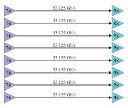
With 20 dB of loss at the 13.3-GHz fundamental harmonic, the channel depicted in Fig. 1 can function with NRZ signaling at bit error rate (BER) < 1E-12, the required 100-GbE bit error rate. But this is only possible if it has optimally tuned equalization at both the transmitter and receiver. At 53 Gb/s—the channel rate required by 400 GbE (Fig. 2)—the fundamental frequency is 26.5 GHz. At 26.5 GHz, this channel has over 40 dB of loss. In the presence of crosstalk, no amount of equalization wizardry can pull NRZ signals out of that noise.
The solution is to pack twice as many bits into each transmitted symbol. While NRZ encodes one bit, either 0 or 1, in each symbol, PAM4 uses four separate levels to encode two bits—00, 01, 10, 11—in each symbol. By encoding two bits per symbol, a 53-Gb/s signal can be transmitted at 26.5 Gbaud with a fundamental frequency of 13.25 GHz.
2. 400 GbE requires a channel rate of 53 Gb/s.
PAM4 achieves satisfactory loss levels, but the cost is an incremental leap in signal complexity. There are 12 distinct symbol transitions with two or three eye diagrams per bit period compared to one for NRZ, and SNR is degraded by at least 9 dB. PAM4 also introduces potential nonlinearities. Variations in the eye heights of the three eye openings is called “eye compression.” Similarly, “timing skew” occurs when the centers of the three eyes are misaligned.
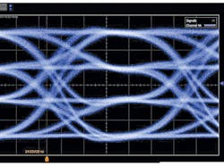
Figure 3 shows an eye diagram that suffers both eye compression and timing skew. Engineers still must contend with jitter, noise, and crosstalk, as well. For these reasons, extremely clean clocks, robust clock-recovery circuits, and sensitive symbol decoders/voltage slicers are necessary. Designers also need better equalization schemes at both the transmitter and receiver to deal with inter-symbol interference (ISI) caused by the channel.
The frequency content of both NRZ and PAM4 signals consist of square-wave harmonics and subharmonics from sequences of identical symbols. The frequency components have precisely coordinated amplitudes and phases. Since PAM4 has four levels, its amplitude-phase-frequency relationships are more complicated than those of NRZ.
3. This eye diagram suffers from both eye compression and timing skew.
Equalization
In Fig. 1, the channel affects the amplitudes and phases of each frequency component differently. By de-correlating its frequency and phase structure, the channel causes ISI. Equalization removes ISI by inverting the channel response. Like everything else, equalization in PAM4 systems is more complicated than in NRZ systems.
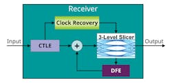
Transmitter equalization, referred to as emphasis or feed-forward equalization (FFE), pre-distorts the signal to compensate for the gross features of the channel response. Two types of equalization operate at the receiver: continuous time linear equalization (CTLE) and decision feedback equalization (DFE). CTLE attenuates low-frequency components and amplifies high-frequency components to compensate for the channel’s low-pass nature. The CTLE typically precedes the clock recovery circuit in the receiver (Fig. 4).
DFE is a type of infinite-impulse-response (IIR) filter that feeds symbol decisions back into the decision circuit. Since PAM4 has four symbols, DFE becomes more complicated but can also provide greater flexibility and the possibility for innovations that could improve PAM4 DFE compared to its NRZ counterpart.
While equalization can compensate for the ISI caused by channel frequency and phase response, it causes problems when crosstalk is present. To compensate for the low-pass channel response, transmitter emphasis and CTLE amplify high-frequency signal components. However, in so doing, they also amplify crosstalk noise. Since DFE operates at the symbol level, it doesn’t affect crosstalk either way.
The parameters associated with ISI, crosstalk, and equalization present a multi-variable optimization problem. It can be thought of as a multi-dimensional design space, where a search is done to locate the point where BER is minimized. S-parameters provide the tools necessary to predict the combined effects of ISI, equalization, and crosstalk.
Modeling
The use of models to optimize and verify designs radically reduces cost and development time. Modeling a system helps find the optimum ISI-crosstalk tradeoff.
Models of Input/output Buffer Information Specification-Algorithmic Modeling Interfaces (IBIS-AMIs) integrate analog simulation with algorithm calculations that run fast enough for designers to try many design variations. IBIS specifies the interface between ASCII files that describe system components and simulation platforms. “Touchstone” files provide the model’s network parameters.
S-parameters are written to ASCII Touchstone files that have the extension .sNp, where N indicates the number of ports. For example, the S-parameters of a single differential channel are stored inAMI extends IBIS so that algorithm-driven serdes subsystems, such as clock recovery, CTLE, DFE, and symbol decoding, can be tested. Other IBIS-AMI input files include the symbol scheme, PAM4 or NRZ, baud rate, signal characteristics, and data pattern. IBIS-AMI models allow analysis to be performed in the time and frequency domains at any point from the transmitter to the interconnect and inside the receiver.
Two IBIS-AMI modeling categories provide different insights. The “statistical flow” processing mode assumes linear-time-invariant (LTI) behavior. While statistical flow offers quick high statistics results, it’s not able to predict nonlinear problems such as voltage compression and timing skew that can plague PAM4 systems. The “bit-by-bit” mode is considerably slower, but it can simulate nonlinearities.
4. Continuous time linear equalization (CTLE) precedes the clock recovery circuit in the receiver.
Certain VNAs, including the Anritsu VectorStar models, feature optional signal-integrity applications that can conduct live updating of eye-diagram simulations from S-parameter data on a sweep-by-sweep basis. Anritsu VNAs also have Advanced Time Domain software to post process S-parameter files to do eye-diagram simulations as well as perform signal-integrity analysis from S-parameter files.
IBIS-AMI Evaluation of Equalization Schemes
Since eye-closure due to ISI varies widely for different sequences of symbols, large statistical samples are needed to evaluate equalization schemes. Fortunately, interconnects are passive LTI systems; therefore, statistical flow IBIS-AMI models can be used.
Clock recovery is challenging because the clock circuit derives the data-rate clock used to time the logic decision circuit from edges in the PAM4 signal. With four symbol levels, those edges aren’t as well defined as in NRZ systems, and nonlinear timing skew aggravates the problem.
A bit-by-bit IBIS-AMI model should be used to check the clock-timing accuracy in the equivalent statistical flow model. The DFE performance relies on the accuracy of the four-level symbol decoder. If there’s timing skew, the DFE taps derived from the statistical flow model come into question and should be confirmed with a bit-by-bit model. With four different symbols to feedback, tuning DFE is more complicated for PAM4 than NRZ.
Most first-generation PAM4 symbol decoders consist of three synchronized voltage slicers, each with its own slice threshold: lower, middle, upper. In IBIS-AMI, the relative timing of each slicer can be offset to determine if a more flexible receiver is necessary for a given transmitter-interconnect-receiver combination.
The accuracy of IBIS-AMI models depends on the accuracy of the .sNp input files. A few simple concepts will help understand the strengths and weaknesses of S-parameter measurements.
Frequency Resolution and Aliasing
VNAs make accurate S-parameter measurements at discrete frequencies. Accurate modeling requires high-resolution S-parameters. Therefore, the step-size (Δf) between adjacent S-parameter frequency measurements should be small.
Another reason to use small spacing is to minimize aliasing. When a discrete function is transformed from the frequency domain to the time domain, the time-domain function repeats, or aliases, in time intervals called the alias-free range, Talias = 1/(2Δf). If the time-delay length of the channel is Tchannel, the alias-free range must be at least Talias > Tchannel, which translates to a step size of Δf < 1/(2Tchannel).
To account for impedance mismatches that may cause multi-path effects, the frequency step size should include at least one point per 90° of return-loss phase-angle change to assure accurate interpolation. The maximum frequency step size should be Δf ≤ 1/(8Tchannel).
Causality
The biggest potential weakness in transforming frequency-domain measurements to the time domain comes from the limited bandwidth of measurement equipment. The Fourier transform from frequency to time requires integration from dc to very high frequency. The trouble comes at the bottom end, because S-parameters can’t be measured all the way down to dc. Therefore, the dc limit of the S-parameters must be extrapolated.
High start frequencies result in causality problems that give the appearance of effects preceding their causes, similar to an output that occurs prior to its input, and convergence problems in the transformation to the time domain. Engineers need VNAs that reduce the causality and convergence risks by getting as close to dc as possible.
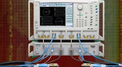
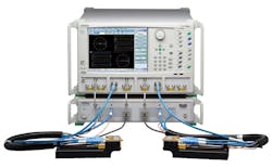
Some Broadband VNAs, like that shown in Figure 5, offer wide single-sweep coverage from a low start frequency of 70 kHz to a high stop frequency of 145 GHz. This ensures that dc extrapolation errors and causality issues are minimized so that simulations match reality.
5. Anritsu’s VectorStar broadband VNAs offer single-sweep coverage from 70 kHz to 145 GHz.
Reciprocity
The S-parameters of passive devices are reciprocal, for example S12 should be the same as S21 in both phase and magnitude. S-parameters measured on VNAs rarely suffer these “reciprocity” problems. One way to estimate the uncertainty of S-parameter measurements is to compare reciprocal S-parameters. If the uncertainty is high, engineers may need to recalibrate.
Reciprocity is a much greater concern for TDT/TDR-based S-parameters. In addition to their timebase jitter and noise problems, the fast rise-time step voltage used by TDT/TDR equipment can cause synchronization problems in the forward and reverse directions.
Passivity
Good lab techniques eliminate passivity problems when measuring S-parameters on a VNA. Assure that the VNA receivers aren’t compressed during calibration and measurement, check that all connectors are in good condition and properly torqued, and verify that any cables used are in good condition and properly de-embedded.
De-embedding and Embedding
S-parameters can also be used to remove the effects of cables, connectors, and traces from measurements via de-embedding. If the S-parameters of everything between the test equipment and the compliance point are measured, the effect of the test fixture can be “de-embedded” to reveal how the signal appears at the compliance point.
De-embedding requires S-parameters measured with dynamic range well in excess of the test fixture’s loss profile; each de-embedded element brings the measurement closer to the noise floor. Because of this, a VNA with 100+ dB of dynamic range can de-embed long backplanes, cables, and traces with higher accuracy.
Embedding is the process of adding the frequency response of a network element to a measurement. Embedding is useful for including the effects of internal components (e.g., equalizers and clock recovery) to determine how a signal will act inside a SERDES.
Accurate COM Requires Accurate S-parameters
At high data rates, it’s not reasonable to expect open eye diagrams at the receiver. As a result, sophisticated tools are required to analyze signal quality. Channel operating margin (COM) is a signal-to-noise-like quantity that combines jitter, noise, crosstalk, and ISI, plus the effects of equalization, into a single figure of merit.
Measuring COM is an involved process based on S-parameters. The differential S-parameters of the channel, Sdd21, are used to calculate the ISI signal impairment and the extent to which it can be removed by equalization. The resulting signal amplitude is given by As.
FEXT is calculated from the crosstalk elements of the system S-parameters. Along with crosstalk and the remaining effects of ISI after equalization, the transmitter distortion, random jitter, and noise are all combined and used to estimate the vertical eye closure defined with respect to a specified SER, Ani. COM is the ratio of the signal amplitude to the vertical eye closure, shown as:
COM = 20log(As/An)
By specifying COM, high-speed standards permit design flexibility. Most standards require COM > 3 dB.
Since COM neglects common-mode noise and NEXT, and approximates the interaction of equalization and crosstalk, it’s not a substitute for a proper model.
Conclusion
The introduction of PAM4 signaling complicates design and test of high-speed components and systems at every step from design to development to manufacture. Key measurements demand accurate S-parameters that can only be measured on high-quality precision instruments such as a VNA.
Charles Tumbaga has a BSEE from San Jose State University. He has worked two years in the electronic calibration/test industry before coming to Anritsu, where he currently serves as product marketing engineer in the Vector Network Analyzer group.
