Optical Switches on Silicon IC Yields Tiny Integrated Spectrometer
The goal of using standard silicon-IC technology to create smaller, better, and possibly less-expensive yet highly sophisticated instrumentation is extending to the optical domain. There’s major interest in doing so for the spectrometer (an optical spectrum analyzer) for two reasons: It’s an indispensable basic tool in optical work, and a high-performance unit is a large and expensive instrument.
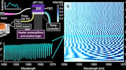
A team at MIT hopes to change that situation by combining IC process technology with electronics and photonic innovation, resulting in tiny spectrometers that may be as accurate and precise as present systems, but with far lower cost, bulk, and power consumption. Furthermore, putting the spectrometer on a chip enables radically different system-level architectures simply not available with a “boxed” unit.
Key to their approach is the use of standard IC-process technology to build all-electronic optical switches that can nearly instantaneously direct a beam of light between the different optical pathways, and these paths can have different lengths. Such switches eliminate the need for the physically adjustable mirrors used in conventional approaches, and results in far more rugged spectrometer. The work is fully detailed in their paper published in Nature, “High-performance and scalable on-chip digital Fourier transform spectroscopy.”
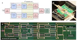
The arrangement uses path lengths in power-of-two increments, and these lengths can be combined in different ways to replicate an exponential number of discrete lengths (Fig. 1). As a result, the potential spectral resolution also increases exponentially with the number of on-chip optical switches. It’s analogous to using a large selection of small weights to precisely gauge a much larger mass.
1. Shown are a block diagram of a generic dFT spectrometer with j switches and K=j/2 − 1 repeated stages (a); photo of the packaged spectrometer with standard fiber interface and a ribbon cable for control and signal read-out (b); and optical micrograph of the 64-channel dFT spectrometer revealing the interferometer layout, thermo-optic switches, and waveguide-integrated germanium photodetector (c). (Courtesy of MIT)
The on-chip digital Fourier transform spectrometer acquires high-resolution spectra via time-domain modulation of a reconfigurable Mach-Zehnder interferometer, a standard and widely used optical arrangement. Increasing the number of path lengths used also boosts signal/noise ratio. Moreover, this configuration also offers advantages over what are called “dispersive” spectrometers that spread the incoming light to characterize its spectral components, with larger spreads (and thus instrument bulk) needed for enhanced resolution.
The MIT design isn’t just a theoretical construct. The researchers used a foundry to build a device with six sequential switches to produce 64 spectral channels, and with built-in processing capability to control the device and process its output (by expanding to 10 switches, the resolution would jump to 1,024 channels).
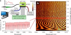
The spectrometer was characterized using a setup (Fig. 2) where the high-resolution transmittance spectra of the device were first recorded by sweeping a tunable laser across wavelengths between 1550 and 1570 nm for all 64 permutations of the switch on/off combinations. The resultant ensemble of 64 spectra yields an m × n calibration matrix.
2. This figure shows the schematic diagram of the dFT spectrometer characterization setup (a); an exemplary transmission spectrum of the dFT device corresponding to an arm-length difference of 0.7 mm (b); and transmission spectra of the device for all 64 permutations of the switch on/off combinations (c). The ensemble constitutes the basis set for spectrum reconstruction. (Courtesy of MIT)
The spectral results don’t “pop out” of the system directly. Extensive calculations, transformations, and correction coefficients are applied to adjust the matrix data and compensate for physical-device realities and defects, including innovative digital-Fourier-transform (dFT) algorithms. The measured performance of the reconstructed spectrum information was close to the anticipated values and detailed the laser wavelengths with ±0.025-nm accuracy.
Whether this approach will prove commercially viable isn’t yet known, of course. Nonetheless, it represents an attempt to leverage conventional silicon-based design and process technologies to provide a new and transformative approach to a long-standing optical-instrumentation challenge. The objective is to simultaneously reduce size, weight, power, and cost, but without compromising performance and even improving it compared to extablished designs.


