Conducting product testing on printed circuit boards (PCBs) has the potential to become costly. Because of this, it’s easy for businesses to view PCB assembly testing as an expense without much value.
So, why test?
The answer is two-fold. First, manufacturers can’t guarantee product quality without testing. Second, when done correctly, testing saves companies time and money in the long term. Inadequate testing can result in inferior quality products getting shipped to end customers, leading to warranty repairs, field failures that require replacement, an inferior product image, and—depending on the industry—even incite potential lawsuits.
On the other hand, adequate testing doesn’t mean that every product requires 100% test coverage. The costs of the tests necessary to achieve the last few points toward 100% are often not only unnecessary, but costly to a point where both production costs and the retail cost of the product can increase exponentially.
It’s essential to assess the optimum amount of testing for a given product and industry to maintain a high-quality product while also limiting the overall cost of test. For example, military and aerospace products require a significantly higher investment in test when compared to other industries due to the nature of their mission-critical operation. On the other end of this spectrum, however, lower-cost consumer electronic products, where some amount of product defects may be acceptable, typically requires a smaller test investment.
Finding Optimum Testing Coverage
Three main elements of a PCB assembly are evaluated during testing: structural devices, structural connections, and functional connections. These elements are assessed using a combination of popular visual, electrical, and functional testing methods, including automated optical inspection (AOI), automated X-ray inspection (AXI), in-circuit testing (ICT), JTAG boundary-scan, and customized test software.
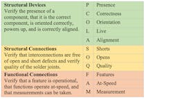
Many PCB assembly manufacturers use an approach known as PCOLA/SOQ/FAM when evaluating the effectiveness of test systems for their products. This approach defines a defect-spectrum of fault categories for assembled PCBs that can be used by test engineers to calculate a score for defect coverage. The “PCOLA” segment of the test evaluates the structural devices of a populated PCB using visual testing methods. This portion of the test looks at presence, correctness, orientation, live, and alignment.
- Presence: Does the component exist? Is it present?
- Correctness: Is the correct component installed?
- Orientation: Is the orientation of the component correct?
- Live: Is the component operational? Does the component respond to stimulus?
- Alignment: Is the alignment of the component skewed or within acceptable tolerance?
The “SOQ” segment uses electrical testing methods to evaluate shorts, opens, and quality. These are connectivity tests to ensure an accurate electrical connection between components as well as identify the quality of those connections.
- Shorts: Is the component connection point incorrectly connected to another connection point?
- Opens: Is the component connection missing a connection to another connection point?
- Quality: Does the component connection conform to quality standards?
Functional testing, which is the last type of test process in the PCOLA/SOQ/FAM defect spectrum, evaluates features, at-speed, and measurement. These tests ensure that components and connections in the system are functioning as expected and measure performance against known benchmarks.
- Features: Is the component feature present?
- At-Speed: Can the component or connection be tested at minimum and maximum speeds?
- Measurement: Can component or connection attributes be measured?
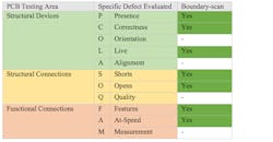
While several testing methods are available, test budgets necessitate manufacturers to select test methods that provide comprehensive coverage of the PCOLA/SOQ/FAM spectrum. A breakdown of the PCOLA/SOQ/FAM approach and the applicable tests can be seen in the table below:
When making decisions about testing and achieving the optimum amount of coverage, it’s important to consider which test methods include a significant portion of the PCOLA/SOQ/FAM defect-spectrum. JTAG boundary-scan, a method for testing PCBs when physical test access is limited, is ideal for this reason. Unlike other methods, boundary-scan can perform tests covering a significant portion of the PCOLA/SOQ/FAM spectrum. Because of this, JTAG boundary-scan testing is often able to reduce or even eliminate the need for additional structural testing methods and equipment:
Other Benefits of JTAG Boundary-Scan Testing
JTAG boundary-scan testing provides a high-level of coverage for PCB testing, but it also offers cost savings in other ways. Equipment acquisition, test procedure development, training, and labor expenses are among the inherent costs of performing boundary-scan testing.
These costs may sound expensive, but performing boundary-scan testing is actually less costly than using popular PCB testing methods like ICT. In fact, in addition to the cost of equipment acquisitions, procedure development, and training and labor, ICT requires test fixture development and equipment maintenance, which are costs that aren’t incurred in boundary-scan testing.
Additional benefits to consider are:
- Significant product yield increase
- Reusable test patterns
- Reduced test time
- Reduced time to market
The Bottom Line
When selecting testing methods, manufacturers must take numerous factors into consideration, including when each method can be deployed, equipment and maintenance costs, and the amount of defect-spectrum coverage. Among the most popular test methods, JTAG boundary-scan testing stands out as the most affordable and versatile option to best meet these factors.
Please contact Rob Steven Williams, Marketing Manager at Corelis for further information.


