Flying Probe Testing: The Fixtureless In-Circuit Test that Must be Fixed
Change in life is inevitable. You know this, yet sometimes you just choose not to accept it. You just close your eyes and think the world has also stopped. But even you realize that’s not the case. It’s for the best that you embrace the change and keep up with it. But have you ever thought why do you keep stalling the change when you know it will happen anyway? That’s because new things are unknown to you, and not knowing things makes them tough to understand.
The flying probe tester is also such a change, which is inevitable but long-stalled. It's one of the most searched topics on Google; therefore, people clearly know about this, but are skeptical about its application. They think it's too complicated, and that’s because it actually is. But again, that shouldn’t stop you from improving your board standards. Before you can absorb what precisely a flying probe tester is, you need to know what makes it so complicated. Maybe it's you, your way of taking it down.
You already know what a PCB is. Whenever anyone says the word, we have a green board in front of our eyes with a lot of conductive traces, pads, drilled holes, and components like resistors, capacitors, etc. PCBs are quite densely populated and hence have critical problems as well. And to solve those problems, in-circuit tests, or ICTs, came into existence. Our topic flying probe tester is one of these in-circuit tests. Before going further, let’s first talk about the basic elements of an in-circuit test.
In-circuit tests check the workings of an application, i.e., white-box testing. Here, we use an electric probe to check the populated PCB for shorts, opens, resistance, capacitance, and other basic qualities. This will show whether the fabrication of the board is proper. There are two ways of performing an ICT: bed-of-nails type of fixture and fixtureless ICT setup.
Bed-of-Nails Testing
Traditionally, “bed-of-nails” testing for a PCB requires a custom fixture to hold the PCB assembly (PCBA) and the pogo pins that contact the PCBA. Like the real-world bed of nails, these devices contain an array of small, spring-loaded pogo pins. Each pogo pin connects with one node in the device’s circuit under test. The probes are held in place by what may be termed a base-board. This is precision-drilled to ensure that the probes are held in exactly the right place for the fixture to make contact with the required nodes on the board. So far, so good.
But again, change can’t be stalled, so the trend in PCBs also changed. And, as a result, there’s an increase in the complexity of the board. This challenges the capabilities of traditional testers. The flying probe extends in-circuit test benefits to applications where this bed of nails is impossible to use (no access), takes too long to build (prototype), or is too expensive to justify (high mix/low volume).
Fixtureless In-Circuit Test or Flying Probe Tester
Traditionally, flying probes worked on bare boards. But from the above statement, we have understood fixtureless in-circuit test (FICT) or flying probe test (FPT) are efficient in PCBs that pose accessibility issues. That’s also the case in prototypes and low- to mid-volume production.
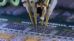
Unlike bed of nails, software instruction is utilized to move the probes. Electromechanical controllers in the flying probe access the PCB. There are four headers on a flying probe tester that test along X-Y axis and can move at a very high speed. It also has a camera to inspect component polarity. The flying probe tester can therefore trim down on the number of test fixtures required. It’s also becoming much easier to introduce changes, especially to features such as a pad or component positions. It takes just a software change.
Again, flying probes usually access component pins directly or through automated test-point probing. They don’t require test points. This improves test coverage over in-circuit tests that use beds of nails. Vias on the board are used as embedded test points. Therefore, the test points are no longer in action.
Elimination of the test points plays a huge role in today’s electronics world. How?
Well, to start with, our electronic gadgets are going from sleek to sleeker, therefore board real estate is a precious commodity. The less the number of tests points, the more the amount of substantial board real estate.
Flying probes have garnered a lot of attention in recent times and that’s not only because of the test points. It’s a method for low volume and for prototype circuit boards for several reasons. Today’s era of increasing board density and complexity poses enough hindrance in programming, but flying probe is easy to program. Low-volume production runs or prototypes don’t really justify the cost of bed-of-nails in-circuit testing, where fixtures are expensive. Using flying probe technology provides a cost-effective solution.
One advantage of the flying probe tester is that the flying probe assembly itself is a precision mechanical item. Thus, it can be placed on small pads or component solder connections with high levels of accuracy. It can also test boards with virtually infinite numbers of nets. This will dramatically decrease the product design cycle and slash time to market.
How Does It Work, Exactly?
After absorbing all of the information provided above, you’re probably wondering what the working principle is for a flying probe tester. It’s the most crucial part of our article and we will try to make it simple. Firstly, imagine that a flying probe works in two different parts: one part is hardware and another one is software.
Let’s take up hardware first.
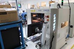
The unit of the device to be tested is sent to the internal tester through a conveyor belt. The probes then contact the vias and test pads, detecting the defects of that unit (if any). It connects probes with drivers such as signal generators and the power supply. The connection is made through the multiplexing system and sensors. There are sensors through which the flying probe tests components of the defective device, like the digital multimeter, frequency counters, etc. When it tests a component, it shields other components on the same unit from the test. This stops the reading from being disturbed.
Shown is the hardware used for a flying probe test. (Source: Sierra Circuits)
As you already know, flying probe testers can test shorts, opens, and component values, and a camera on the tester inspects component polarity as well. Therefore, it becomes much easier for the tester to test for several aspects of a PCB in a single test.
Programming
As for the software or test program, the flying probe tester carries out programming more easily and more quickly than traditional ICT. Let’s find out why and how.
We assume you have at least a vague idea about CAD—the design files that are provided by engineers. These files aren’t compatible with flying probe test programming. Therefore, for the sake of execution, the tester first transforms CAD data into an applicable file. Then, reference data points conforming to the defective unit should be picked up from CAD data. Subsequently, the newly generated file runs through a test program—it’s run with new files with corresponding formats generated. Lastly, all of the files created cater exactly to that unit’s test demands and requirements.
Once the program is ready, the probe tester gets into action, which comprises obvious things like testing for shorts, opens, isolation, and so on. As soon as a unit gets fixed on the platform, the programming will be carried out to inspect the fabrication or assembly issues. We can now debug the flying probe test much earlier than a conventional ICT test. One thing to keep in mind: Debugging should be done prior to official testing.
Let’s now go over testing through the probes.
Phase Difference Measurement Unit
In today’s world, the last thing that we have is time. Isolation tests can be really tricky and time-consuming, but we have solution tests for that, too. The phase difference measurement (PDM) unit is one such test. PDM sends a high-frequency signal between the reference line and signal line to measure differences between these phases. This will cut down unnecessary isolation tests within a net.
High-Voltage Stress Test
You might know there can be high-resistance defects that can go undetected in the above process. The good news is the high-voltage stress (HVS) test targets the high-resistance, undetected isolation defects by PDM. We conduct HVS by applying high-voltage pulses between signal lines to detect high-resistance defects. HVS and PDM are similar with respect to the fact that both inspect each net once. Thus, it works rapidly.
When we say high, that includes the range from high to higher. The maximum applicable voltage with standard isolation resistance measurement is 250 V. This offers the option of applying a maximum of 500 V/1000 V. For the super-high-resistance isolation defect, a low-power test voltage is applied. The usage of low voltage allows users to conduct a super-high-resistance test without adding high stress on the tested boards.
Micro Shorts Detection
The sudden application of a high voltage in isolation tests may cause burning out of parts containing micro shorts. This is due to carbonized residue possibly reacting with moisture in the air or gases in the factory, causing the element to relapse as a high-resistance short error after the test is complete.
Micro-short tests can avoid such damage and trouble by applying a low voltage before gradually increasing the applying voltage. Sometimes, a high-resistance short between multiple layers of a board possesses the characteristics of semiconductors and capacitors. The reversing of polarity of high voltage could also detect these defects.
Introducing anything new into a system that’s working fairly effectively is rather tough. But once you take the leap of faith, things might go from fair to great. The existing ICT isn’t obsolete, but introducing flying probe testing can improve your boards in multiple ways. From real estate to time to market of PCBs, it even cuts down on unnecessary isolation tests. Whether it’s ease of programming or minimizing repetitive tests or for the other reasons mentioned here, flying probe is the best solution to many problems you face right now.
Taisha Chattopadhyay is a Technical Content Writer at Sierra Circuits.


