“Load Slamming” Can Help Save Cost When Optimizing Output Capacitance
The previous article in this series discussed types of testing that can potentially be performed with load slammers. In this last installment, we show some scope plots of actual testing using a load slammer, along with commentary on what those waveforms can tell us.
The voltage regulator used for these tests is a dual-phase buck regulator with an input voltage of 12 V and output voltage of 1.50 V. Operating in current mode, loop bandwidth is approximately 40 kHz with phase margin exceeding 80°.
Since this board did not have a slammer connector, the slammer was directly soldered to the board with minimal connection length. Distance from the slammer to output capacitors was 10 mm or a bit more, with a 10-μF ceramic next to the slammer. Output voltage measurements were taken from the regulator board, and current measurements were taken from the slammer.
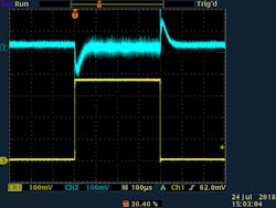
To start transient testing, the slammer GUI was adjusted for a positive current pulse of approximately 400 μs (Fig. 1). This was chosen based on the loop bandwidth of the regulator and shows a full step and release response.
1. Initial setting: Blue = V(out), Yellow = I(out) @ 75 A/V.
What can we learn from this plot? Here are some thoughts:
- Current step is 0 A to 28 A, which is a reasonable value for exercising a 32-A converter.
- There’s ringing on both step and release, which is above the loop bandwidth. This will be related to output decoupling and is discussed later. Averaging is used to get out some of the switching noise so that we can better see what’s happening.
- The pulse is wide enough to provide time for a full response, returning to steady-state operation.
- Step and release waveforms are essentially identical, indicating that the converter response is small-signal dominant. Large-signal inductor slewing isn’t an issue.
- There’s no ring in the loop response, which is consistent with high loop phase margin.
- The slammer current waveform is crisp and square, facilitating a clean and repeatable step response. There’s little current ring and no tilting or decay as with some load units.
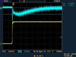
Figure 2 zooms in on the initial step to see it in more detail. Maximum undershoot is 114 mV (7.6% under) for load step.
2. 28-A load step: Blue = V(out), Yellow = I(out) @ 75 A/V.
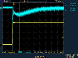
Figure 3 looks at response time.
3. Load step: Blue = V(out), Yellow = I(out) @ 75 A/V.
What can we learn?
- Step response is 9.8 μs to maximum undershoot. This is about 2.2 times the loop time constant (based upon the known 40-kHz loop bandwidth).
- Recovery to steady state is roughly 50 μs later.
- Recovery time largely depends on the integrating capacitor in the feedback loop. Reducing the integrating capacitor value will reduce recovery time if phase margin is still good.
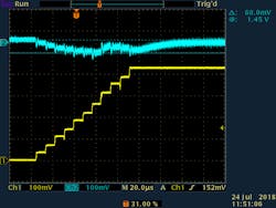
Next, let’s discuss slew-rate implementation as it relates to slammers. Figure 4 shows a 32-A step, but with a reduced overall current slew rate, realized using discrete smaller current steps.
4. 32-A stepped slew: Blue = V(out), Yellow = I(out) @ 75 A/V.
While this method may appear coarse, it has some distinct advantages:
- It’s much easier and less expensive to implement than a variable analog slewing circuit.
- It’s more accurate on a macro scale because the step sizes and timing are known and controlled.
- It’s easy to implement and adjust with a microcontroller via GUI and USB interface.
Using this method to slow the current slew rate allows us to learn more about the how slew rate affects transient response:
- 32 A is stepped in approximately 88 μs for a slew rate of 0.36 A/μs.
- Undershoot is only 60 mV (4.0% under), which is much lower than our previous 28-A response. Why the difference?
- The slower di/dt allows the regulator loop to respond as the step is slewing. Conversely, if load slew-rate requirements are low, it’s easier and potentially less expensive to design a regulator that can meet those requirements.
- This demonstrates the usefulness of having a variable slew rate.
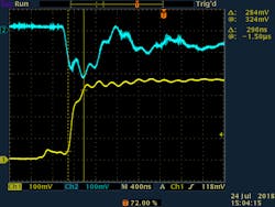
Lastly, let’s discuss the ring seen in earlier scope plots and how it relates to load current slew rate. As seen above, the variable rate is accomplished with a series of smaller steps getting ever closer together. When the steps narrow sufficiently, they begin to disappear, and the waveform becomes analog. Ringing occurs due to parasitic circuit elements, both in the slammer and the load. Figure 5 shows a load step of roughly 93 A/μs.
5. 93-A/µs load step: Blue = V(out), Yellow = I(out) @ 75A/V.
At this rate, we are well beyond the loop and looking at the output decoupling solution of the voltage regulator. Output voltage deviation is 240 mV.
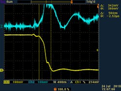
Figure 6 shows a load release slew rate of 55 A/µs.
6. 55-A/µs load release: Blue = V(out), Yellow = I(out) @ 75A/V.
Output voltage deviation, off the screen in Fig. 6, is about 300 mV. Here are some final observations:
- Output voltage rings at around 830 kHz on both step and release. It would calculate to the 10-µF ceramic ringing with 3.7 nH of inductance. This is very possible given the board trace length to output bulk capacitors and ESL (equivalent series inductance) of the polymer output capacitors.
- There’s an additional ring on the step edge of approximately 4.5 MHz, possibly due to the faster edge in the step waveform.
- There’s no input capacitance on the slammer other than parasitic MOSFET capacitance. This allows for extremely fast response, but it can also ring, depending on the regulator output impedance. Care should be taken to minimize the distance between the slammer and voltage-regulator output decoupling.
- A more complete regulator output filter solution (more ceramic capacitors near the output or shorter traces) will likely reduce output voltage deviation and ringing. Thus, the slammer can supply useful information well above the loop bandwidth.
In summary:
- Load slammers are low-cost, affordable instruments, as opposed to expensive, calibrated, full-featured load systems.
- They are effective in measuring transient response of board-level converters.
- They corroborate testing with other instruments (such as Bode analyzers) and with simulation.
- They can also provide some level of loop information independently. The latter includes response time (related to loop bandwidth), recovery time (related to integrating capacitor value), and very approximate phase margin.
- Slammers can help distinguish between small-signal dominant and large-signal dominant responses.
- Slammers can exercise a voltage regulator consistently and repeatably. Step size can start small and benign, increasing to beyond what the actual load may require. This helps test for margin in design.
- Variable current slew rates show how regulator response can vary, depending on load requirements, aiding in optimizing regulator design.
- Very fast slew rates can provide useful information regarding the regulator output decoupling solution.
It’s my sincere hope that you find tthis article series helpful for your design and testing efforts. Don’t be afraid to experiment and probe to learn more about your voltage regulator—its good points, bad points, transitions, and limits.
Now have fun and go slam some loads!
For more on the LoadSlammer, go here.
Roger Beeston is the Founder of ProGrAnalog.

