Getting a Handle on Power-Rail Measurements
Download this article in PDF format.
Most of today’s electronic designs require many different supply voltages to function properly. Even within the same circuit, many components require multiple voltage levels. This is especially true with highly integrated system-on-chip and microprocessor designs in which multiple technologies interface together.
As systems become faster and more complex, engineers must take the time to thoroughly test power rails to ensure that each part of the system is receiving the correct power to meet its needs. A number of trends are conspiring to make this more challenging, including:
- Power-efficiency features such as power gating and dynamic voltage and frequency scaling (DVFS)
- Dynamic loads with fast transients
- Increased crosstalk and coupling
- Switching regulators with faster rise times
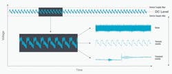
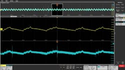
When testing power rails, it’s important to look at each dc line to see if the power supplied is within the tolerance band of a target system or device. This includes the nominal dc value of the line, as well as any ac noise or coupling present. The ac noise in a power-rail signal can be broken down further into broadband noise, periodic events, and transient events (Fig. 1). All three of these noise sources impact the quality of power that reaches a device, and it’s important to reduce these noise sources to the point that the target device can operate correctly.
1. The ac noise in a power rail includes broadband noise, periodic noise, and transient events.
Before you can minimize these noise sources, you need to be able to see and measure them accurately. Major factors to consider when performing power-rail measurements, which we will discuss in more depth, include bandwidth requirements, system noise and additive probe noise, tradeoffs of ac or dc input coupling, and loading challenges for power rails.
Bandwidth
When looking at many power-delivery designs, it might seem that measurement system bandwidths of a few tens of MHz are enough. Most switching designs switch in the hundreds of kHz up to perhaps a few MHz. In the past, larger physical designs and devices that ran off higher supply voltages were less sensitive to noise, and noise content above 20 MHz was rarely a concern.
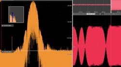
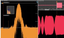
Now, however, as design sizes and supply voltages shrink, tolerances follow. Power-distribution networks are analyzed more as transmission-line environments for factors such as cross coupling, line impedances, and resonant regions. In Figure 2, Channel 3 (red trace) is a capture of a power rail that has high-frequency interference coupled onto the line. If this energy is too large, it may interfere with the operation of the device or even cause damage.
2. High-frequency interference can disrupt the operation of a device.
Note also that the fundamental switching frequency of power-conversion devices may be relatively slow, but the edge speeds and rise times are typically much faster to help reduce switching loss. These edges and other interferers can excite the power-distribution network in a way that generates noise and harmonics at much higher frequencies. Depending on the target device and the function of the circuit, such higher-order harmonics can interfere with operation. Choosing an oscilloscope and probe with enough bandwidth to see these events is crucial to diagnose problems related to high-frequency interference.
Probe Connections
The connection to the device under test (DUT) is the single biggest driving factor in getting quality measurements. Connections that offer low inductance paths to ground and have minimum effective capacitance will reduce ringing as well as provide the most bandwidth. These connections are typically implemented with either solder-in adapters or high-performance connectors. Micro coax and flex solder-in adapters offer a semi-permanent connection to DUTs when repeated tests need to be done on an unplanned test point.
While these connections provide the best signal integrity, they’re also not always convenient, as they require modifying the target device or planning for test points when designing the system. In such cases, browsers and adapters can be used with the caveat that most browser accessories derate the bandwidth of the system. For instance, flying lead square pin adapters don’t usually have more than a couple hundred MHz of effective bandwidth. This is reduced more when adding clips and other connection aids.
The last thing to consider when choosing a connection method is the test environment. Many system validation engineers need to test designs in extreme temperatures. Specially designed extreme temperature cables and solder-in tips support testing devices from −55 to +155°C.
Managing Ambient Noise
As supply voltages become smaller, due in part to shrinking process geometries, low noise measurements are required to see the small variations present on dc supplies. In addition, many designs are focusing more stringently on power integrity. In turn, that means tighter tolerances for each supply. To measure this, not only does the oscilloscope need to have extremely low noise, but any probe connected to the oscilloscope should contribute as little noise as possible to the measurement.
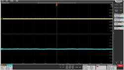
Taking noise measurements of both the instrument and the attached probes provides a baseline for total system noise performance. Simple measurements like peak-to-peak and RMS of the voltage present at the inputs when no signal is applied offer a quick way to compare the additive noise of the probing system. In Figure 3, Channel 1 (yellow trace) is an oscilloscope channel with no input while channel 2 (blue trace) is a power-rail probe with its input shorted. In this case, at 1-GHz bandwidth, the probe is adding just 17 µV of noise to the oscilloscope input.
3. A noise measurement of the oscilloscope and attached probes provide a baseline for total system noise performance.
Passive Probe Challenges
High-attenuation probes offer great dynamic range when looking at a wide variety of signals. However, due to the attenuation, they often introduce more measurement noise compared to low-attenuation probes. This is seen in Figure 4, which compares a 10x passive probe to a probe designed for low-noise and power rail measurements. In this example, the passive 10x probe (blue trace) shows 157.1-mV peak-to-peak noise compared to 38.7-mV peak-to-peak for a probe designed for power-rail measurements.
4. The blue trace shows the 157.1-mV peak-to-peak noise of a traditional 10x passive probe compared to 38.7-mV peak-to-peak for a power rail probe such as the Tektronix TPR1000.
The problem with high-attenuation probes stems from the fact that the signal is divided by the attenuation factor, driving it closer to the noise floor of the measurement system. This is shown by calculating the signal-to-noise ratio (SNR):
For example, if we choose an input of 10 mV and a random noise specification of 200 µV (this specification can be found on the datasheet of your oscilloscope as random noise, typically in units of Vrms), then a 10x probe’s SNR would be:
A low attenuation 1.25x probe, on the other hand, would have an SNR of:
Vertical Scale and Noise Performance
The noise performance of an instrument scales with the vertical sensitivity setting—higher sensitivity ranges offering better noise performances than lower sensitivity ranges. Maximizing the displayed signal on screen will provide more resolution and a more accurate representation of the signal by the instrument.
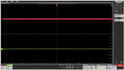
Lower vertical sensitivity ranges can often make signals appear to have more peak noise on them than they really do (Fig. 5). In this example, both channels have nothing attached to the input. Channel 3 (red trace) at 1 mV/div has 521.2-µV peak-to-peak noise versus channel 4 (green trace) at 100 mV/div with 8.953-mV peak-to-peak noise, approximately 17 times more reported noise than channel 3. Note that the 8.953-mV setting on channel 4 is <1% of the full-scale voltage.
5. The example demonstrates how noise performance of an instrument scales with vertical sensitivity settings.
On some oscilloscopes, it may be possible to further reduce noise by using waveform averaging to produce higher resolution samples. This is done by applying finite-impulse-response (FIR) hardware filters based on the current sample rate. These FIR filters maintain the maximum bandwidth possible for a given sample rate while rejecting aliasing.
DC Offset Challenges
Many designs have a bulk supply voltage that filters down through various dc-dc converters to the needed supply voltages required by the various ICs and systems. Often, the bulk supply voltage is many times higher than the voltage needed by ICs.
For example, vehicles convert 12 V dc down to the sub-1-V supply voltages needed to run the processors in the infotainment and safety systems. It’s also not uncommon to see data centers supply power to servers via a 12-, 24-, or 48-V dc supply that then gets converted down to other supply voltages on the motherboard. Being able to look at every link in the chain from supply output to IC pin can help identify noise that’s being transferred from other voltage domains.
Therefore, it’s important to choose a probe that offers enough offset to look at all of the rails being tested in a power-delivery network. This is difficult because many oscilloscope front ends limit the available offset depending on the vertical sensitivity selected. At lower volts per division-settings, the instrument will have less offset. High-attenuation probes usually have more offset capability, but, as discussed previously, they have more noise than low-attenuation probes.
Dealing with dc offset can be avoided by using the ac coupling of the scope, which removes the dc component of the signal. However, doing so obscures any low-frequency events that may be happening, such as voltage droop. As shown in Figure 6, ac coupling hides low-frequency information like voltage-line droop or creep as the load changes.
6. The ac coupling removes the dc component of a signal, but obscures low-frequency events.
Ideally, enough dc offset can be added to the input signal to permit the use of dc coupling, which offers a more complete picture of a device’s behavior. Power-rail probes are specifically designed to add enough offset range to the oscilloscope/probe system to support dc coupling on most power rails. Look for probes with at least ±60 V of dc offset to cover the most common standards in automotive, industrial, and data-center applications.
Minimizing Loading
The challenge with probing power rails for making power-integrity measurements is choosing a probing method to see the high-frequency ac content on the dc supply, while also taking care to not load the dc portion of the signal so much that it interferes with device operation. High-impedance probes offer the best loading for dc situations. However, they often have excessive noise or don’t have the bandwidth necessary to see the high-frequency events that are of interest while also dc coupling the signal. A 50-Ω transmission line offers excellent loading for high-frequency signals on a power rail, but it acts as a low-impedance voltage divider for dc signals.
The ideal probe for making power-rail measurements would supply very high resistance at dc and a 50-Ω transmission line at ac. Here, you’ll want to consider probes with high 50-kΩ dc resistance and the ability to transition to 50 Ω at higher frequencies. Such probes offer the best of both worlds and avoid the limitations of other probing options.
Power-rail analysis is one of the most important tools for engineers to master as the need for power integrity continues to rise. With the suggestions provided here, engineers can overcome the measurement and connectivity challenges faced when analyzing and verifying dc supplies.
Austin Hall is an Application Engineer at Tektronix.
