This article is part of the TechXchange: Delving into EMI, EMC and Noise
This file type includes high-resolution graphics and schematics when applicable.
What is a myth? A myth is defined as a popular belief or tradition that has grown up around something; an invented story, idea, or concept; an imaginary or fictitious thing; an unproved or false collective belief. Many myths circulate through the field of electromagnetic interference and electromagnetic compatibility (EMI/EMC), some of which are untrue, or only partially true, or based on misunderstanding. Most of these myths came about based on attempts to balance reality (accuracy) versus the time and cost spent on successfully solving EMI/EMC issues.
Myths provide a way to obtain quick answers that are not necessarily accurate, but give us rough estimates. Many of these myths were generated simply to make them easy to remember. The intent of this article is to explore some of these myths and provide explanations and clarifications to the reader.
1. EMI/EMC is “black magic.”
This is probably the most well-known and most common description about EMI/EMC that I’ve heard from engineers and designers in my 40-odd years working in this field. We often use the terms “black magic” or “black art” when describing an unexpected or unusual result. These phrases are used to describe results that we don’t understand or can’t comprehend or even can’t make sense of. It’s understandable, then, that this phrase could be applied to some aspects of EMC.
After some EMI mitigation work, the result often is contrary to what we expected and sometimes actually counterintuitive. For example, shielding against magnetic fields using thin conductive materials with a relative permeability of just 1 seems like magic, but has a simple explanation if one knows the frequency of the magnetic field.
So, the major reason EMC is seen as “black magic” is the lack of understanding in the fundamental principles of electromagnetics. Also, the coupling mechanism in an EMI problem may not have been completely identified, or a number of coupling mechanisms may have been at issue. Often the paths that RF currents take aren’t always obvious, and distributed parasitic components in a circuit may have been ignored. Commonly, many sources of emissions exist and when the most predominant one is minimized, then the second one in line will predominate. This often means that the initial fix will be less effective than expected; not that it won’t work.
2. Cable shields are only connected to ground at one end.
When a shielded cable is connecting two pieces of equipment, engineers were always told that the shield should be connected to chassis or ground at only one end. The most common reason given to do this is to avoid ground loops.
Cables routed over long distances will cross different ground potentials that may exist. This difference in ground potentials will create a noise current flow in the cable shield. Audio engineers especially do not like this situation. It results in electric field shielding with only limited plane wave shielding and very little magnetic field shielding. When it comes to high-frequency shielding, the shield must be grounded at both ends.
For the cable shield to be effective when grounded at both ends, one must first avoid using the shield as a return path. High-power and/or RF currents should be routed on separate and dedicated return conductors that are isolated from chassis. If the noise currents on the shield are dc or at power frequencies, then an RF capacitive ground connection to the enclosure will shunt RF currents but present a high impedance to the low frequencies and avoid the dreaded audio-frequency ground loop.
Another approach is to use a differential signal and receiver set. In this situation, the voltage induced in the center conductors as shown is common mode and will be reduced by the common-mode rejection ratio (CMRR) of the receiver.
3. To meet EMI requirements, we only have to put the equipment in an all-metal enclosure.
This particular EMI myth ignores the radiation from cables entering and exiting the enclosure as well as the weak link in an enclosure, namely seams and apertures. When PCBs are contained in an enclosure, the fields generated by the PCBs set up noise currents on the inside walls of the enclosure. This noise current flowing on inside surfaces can then flow out onto the external surface of the enclosure through any seams or apertures, causing radiation. It’s this “inattention” paid to seams and apertures that can result in radiated emissions and immunity/susceptibility failures.
Therefore, limit the size of seams and openings in the enclosure. Generally, avoid openings approaching the half-wavelength of an offending frequency. Also, when a shield is terminated on the outside of the enclosure, the noise current will flow onto the shield, which causes radiation, too.
When going from an unshielded enclosure to a shielded enclosure, it may change the frequency of maximum radiation. To meet low-level radiated emission limits with a shielded cable, the signal return currents on the shield should be avoided whenever possible or limited in magnitude. Often, in a thick enclosure, gaps may appear between fasteners. It’s the length of the gap, the dc resistance, and the frequency-dependent contact resistance that limit the enclosure’s shielding effectiveness.
4. All conductive coatings or plastics are the same.
Many manufacturers quote shielding effectiveness of conductive coatings only for plane wave fields, which are relatively easy to shield against. The engineer must determine what type of field is dominant in the product, whether plane wave, electric field, or magnetic field.
A low-conductivity (or high-resistance) coating such as carbon may be effective against an E field, but not very effective for a magnetic field or plane wave. In reality, it’s often required to achieve plane-wave and magnetic-field attenuation, which in this case means a high-conductivity (or low-resistance) coating. The engineer must compare the performance of a pure metal plating, conductive paints, and/or conductively loaded plastic to determine the difference in shielding between different materials and if it meets shielding-level requirements. The most prevalent problems when using conductive paints/coatings are incomplete coverage and failure to bond the conductive coating at the seams.
5. A capacitor’s impedance will keep decreasing with increasing frequency, OR an inductor’s impedance will keep increasing with increasing frequency.
These statements are only true for ideal components. A real capacitor will have a parasitic equivalent series inductance (ESL) and inductance from the connecting wires or PCB traces, as well as parasitic resistances (ESR) (Fig. 1). A series resonance circuit is formed by the LCR series components.
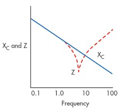
When the capacitor is connected across a signal line, its impedance will decrease with increasing frequency; the impedance will be at a minimum at resonance, rather than at some high frequency. At resonance, the impedance will be lower than the capacitive reactance alone (Fig. 2).
This effect can be useful when an EMI problem frequency is known, since a low impedance can be achieved at the resonance frequency with a lower-value capacitor when the inductance is deliberately increased. A low-value capacitor may be useful in minimizing attenuation of the intentional signal. Above resonance, the impedance of the capacitor begins to increase with increasing frequency due to its ESL. To achieve lower impedance over a wider frequency range, a number of capacitors with different resonant frequencies may be placed in parallel.
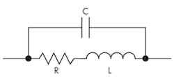
A practical inductor with more than a ½-turn winding will have a parasitic or interwinding capacitance between the windings and resistance associated with the wires used in the windings (Fig. 3). Because the capacitance is in parallel, a parallel resonance circuit is formed by the LCR components.
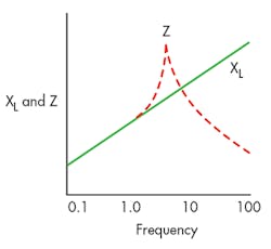
When an inductor is connected in series with a signal line, the reactance will increase with increasing frequency, and the impedance will be a maximum at resonance rather than an infinitely high frequency (Fig. 4). At resonance, the impedance will be higher than the inductive reactance alone.
Just as for the capacitor effect, this inductor effect can be useful when an EMI problem frequency is known, since high impedance can be achieved at the resonance frequency with a low-value inductor when deliberately increasing the capacitance. A low-value inductor may be required to minimize attenuation of the intentional signal. Above resonance, the impedance of the inductor begins to decrease with increasing frequency due to the capacitance.
6. A commercially purchased power-line filter will perform in the equipment as specified by its datasheet.
Still another common mystery of EMC is why a power-line filter with an impressive level of specified attenuation doesn’t perform as specified when wired into the real system. When a manufacturer of an inexpensive filter specifies a level of attenuation, the attenuation must be determined if it’s specified for common-mode (CM) noise or for differential-mode (DM) noise.
Most commercial-type power-line filters only include a CM inductor and a capacitor across the line for the DM noise. Thus, for DM noise, only the capacitor is effective, while the inductor is only effective for CM noise. Figure 5 shows a typical commercial filter schematic. Even the most inexpensive filter is tested to an MIL-STD-220 test method.
The majority of signal generators are designed for a 50-⦠load, and the subsequent measuring instrument usually has a 50-⦠input impedance; both are single-sided. MIL-STD-220 specifies a 50-⦠load and source impedance, which is achieved with an input attenuator. In the MIL-STD-220 test method, the input attenuator exhibits a series resistance, which effectively damps the resonance of almost any filter; also, an insertion gain isn’t seen in the attenuation curve.
MIL-STD-220 allows either a CM or DM measurement. The manufacturer may not mention this, so it’s essential for engineers to know what type of noise (DM or CM) they are experiencing and what level of attenuation will be required. The load impedance on a filter is rarely 50 â¦, even on 120-V ac power lines.
When the filter is used for dc power, the load impedance is typically 1 to 20 â¦, which changes the filter’s attenuation characteristics. Also, the source impedance of the noise voltage may not be 50 ⦠as used in the MIL-STD-220 test. On top of that, the MIL-STD-220 test method doesn’t require a power current to flow in the filter during the test. If the filter does contain DM inductors and is used on dc power, then the value of the inductance may be different (typically lower) with dc current flowing.
For these reasons, the attenuation achieved in the real world will be different from the datasheet and often lower. The ideal filter testing is custom-designed for the EMI test source impedance (typically an LISN) and uses the real switching power supply intended for the product operated at the anticipated current draw.
7. Along the same line, a power-line filter tested alone with a power supply will be just as effective when mounted in the final system enclosure.
An unshielded power-line filter with unshielded input power lines can have system noise coupled to both the filter components and the input connections to the filter. This is most likely when the filter components are mounted on a PCB containing noise sources like switching power supplies or digital logic. The problem may be exacerbated when the input power is routed some distance away from the intended load. If the noisy output side of the power supply is run close to the filtered ac input power-line side, then the resultant crosstalk can either reduce the filter attenuation or even negate it completely.
Very often, an effective filter capable of meeting all EMI requirements will fail conducted emission tests when unshielded and mounted on a PCB, or the input/output power lines are harnessed together. If the input power lines to the equipment enclosure are unshielded, a PCB-mounted filter may also result in a failure in radiated emission measurements.
Ideally, the power line filter will be shielded and mounted on the equipment enclosure wall with the input power connector mounted to the filter enclosure. Furthermore, a filter with a built-in connector should be mounted inside the enclosure with the connector facing the outside. If this isn’t feasible, then a shielded filter should be mounted as close to the input power connector as possible using shielded wires, if possible, to connect between the connector and the filter.
8. Going to a four-layer PCB will always reduce EMI.
Measurements made on differential signal traces and single signal traces above a ground plane in both a microstrip and stripline configuration (Fig. 6) showed the following: The differentially driven stripline PCB has a lower level of emissions only at certain frequencies when compared to two differential traces close to and over an image plane (a ground plane underneath the traces). At high frequencies, the level of emissions is similar for both configurations.
Other comparisons between differential stripline and differential traces with an image plane also show that the stripline radiates at a lower level. Because the emissions from the stripline are so low, emissions from connectors, short lengths of single traces outside of the stripline, and the various ICs will predominate. When the major source of radiation is the PCB and not components, observation of numerous PCB layouts has shown that the radiation from a PCB, with full upper and lower ground planes tied together with a number of vias, is invariably lower than a PCB with a single ground plane. So, be wary of using noisy components.
However, errors in signal routing can also result in radiated-emissions failures. This is especially true for high-speed traces. Any breaks in the ground-plane return path can cause a generation of an RF voltage through this high impedance, causing common-mode noise generation throughout the entire board. Therefore, adding more ground planes does not necessarily reduce the emissions of the PCB.
Moreover, a PCB with an overall ground plane and an incomplete second ground plane with small islands is only slightly more effective than a PCB with a single ground plane when the islands are connected to the overall ground plane using a number of vias. When a ground plane is quoted as having an impedance in the microhms, this refers to its dc intrinsic or metal impedance. It’s the impedance seen by an incident electromagnetic wave.
However, when the ground plane forms a path for RF currents, due to its mutual inductance, the impedance will be much higher. For example, the impedance of a 12.6- × 10-cm copper 1 oz. ground is 0.64 ⦠at 2 MHz when the signal trace is 1 cm above the ground plane, and 0.045 ⦠when the signal conductor is 1 mm above it.
9. A PCB should only be grounded in one place.
Single-point grounding is used to prevent common ground impedance circuit coupling. That is, the entire circuit system is regarded as a structural ground reference point, and all of the ground connections are connected to this point.
Single-point grounding is divided into two types: series and parallel. Because the series type generates common ground coupling, it’s better for the low-frequency circuit to use parallel single-point grounding. To prevent power frequency and other interference from stray current in the signal ground line, signal-ground and power-ground paths should be isolated from the ground and the chassis, and only connected on the safety ground bolt to earth ground wire by power ground or chassis ground (except floating).
High operating frequency (>30 MHz) should use multi-point grounding. That is, in this circuit system, a ground plane is used to replace the respective ground loop for each part in the circuit. Because the ground lead inductance and the frequency and length are proportional, the high operating frequency will increase common ground impedance, which will increase electromagnetic interference generated by the common ground impedance. Thus, the length of the ground line should be as short as possible. When using multipoint grounding, try to find the nearest low-resistance ground plane to ground.
Working frequencies between 1 and 30 MHz use mixing grounding. When the length of the ground wire is less than 1/20 of the operating signal’s wavelength, single-point ground is used. Otherwise, it’s multipoint grounding.
Why do you want multipoint grounding for high-frequency systems? Basically, RF fields generated from a PCB can and will couple to a metallic structure, such as the chassis enclosure. As a result, RF eddy currents will develop in the structure and will circulate within it, creating a field distribution. This field distribution may couple to other circuits. These eddy currents are then coupled to the card cage through distributive transfer impedances and then through attempts to close the loop by coupling back to the backplane.
If the common-mode reference impedance between the backplane and the card cage isn’t significantly lower than the distributive "driving source" of the eddy currents, an RF voltage will be developed between the backplane and the card cage. In other words, the common-mode spectral potential between the backplane and card cage must be shorted out. This may take the form of frequently connecting the backplane ground plane to the card cage (chassis) at regular intervals around the perimeter of the backplane.
10. Adding a ferrite core or balun on a cable will always reduce radiated emissions.
If no current probe is available, adding a ferrite on a cable is often used as a diagnostic tool to determine if an RF current is flowing on the cable. If a cable is electrically long (greater than ½ wavelength), then the current on the cable is at maximum at some location and zero at another. If a ferrite balun is placed on the low-impedance section, then any RF current within the frequency range of the ferrite will be reduced due to the impedance of the ferrite. However, when placed at a high-impedance section, the current will not be reduced. Therefore, move a ferrite up and down the cable to ensure that a low-impedance section is found. A ferrite on a cable or wire also acts as an effective receiving antenna.
If a ferrite is located on a PCB close to a source of high-level RF, such as a clock oscillator, switching power supply, or digital ICs, the fields generated by these devices may couple to the ferrite and inject current into the cable and wire. In this case, adding the ferrite is counterproductive.
If CM RF current flows on a number of wires or cables in close proximity to each other, then baluns are required either on each conductor, including signal and power grounds, or overall. A common mistake is to put the dc power through one balun and the return through another. The resultant DM current can saturate the ferrite, making it ineffective.
When signal and returns are placed through the same aperture in the ferrite, the balun will not attenuate DM signals up to 1 GHz. However, when the signal is routed through one hole in a two-hole balun and the signal return through another, attenuation of the signal is seen at much lower frequencies. Adding a ferrite core or balun on signals and returns together thus will not affect a DM current, but will attenuate a CM current.
11. Adding filters to PCB I/O signal lines will reduce radiated emissions.
Adding a low-pass filter will attenuate DM noise appearing between a signal and signal ground. To reduce CM noise, the capacitors must be connected to a clean, typically chassis, ground. CM noise appears on every conductor on a PCB including the ground (signal return). When the capacitor is connected to a noisy digital ground, then the currents are conducted via the capacitor to the signal lines. Removing the capacitor may actually decrease the common-mode currents on the signal lines.
If individual inductors are used, then they will attenuate the desired DM signal. If the inductor is wound, preferably bifilar, then it will not attenuate the DM signal up to typically 1 GHz, but rather attenuate the CM currents.
However, some reduction in CM currents on all of the signal lines can be achieved by connecting the noisy digital ground to a clean, typically chassis, ground. If the noise currents are predominantly CM, then a common-mode choke, sometimes referred to as a balun, is available in many different configurations.
It’s important to use a balun that has a high impedance at the frequencies of concern, as well as the correct ferrite material; otherwise, a multi-turn choke must be chosen. If a multi-turn component is used, then the impedance will reduce above its resonant frequency. Also, if the signal lines are in a cable external to a shielded enclosure, the connection to chassis/enclosure ground should be as close to the point where the cables exit the enclosure as possible.
Read more articles like this at the TechXchange: Delving into EMI, EMC and Noise


