Switch-Mode Power Supplies for Beginners: An Efficiency Primer Part 1
This file type includes high-resolution graphics and schematics when applicable.
Power efficiency is a fundamental characteristic of any switch-mode power supply (SMPS), and its measure generally dictates the quality of the conversion device. High numbers bestow bragging rights upon the successful engineer, while low numbers usually denote the need for modification or redesign.
Maximum efficiency is a prime consideration for all SMPSs, but even more so for those found in portable devices, where battery life must be prolonged to offer consumers extended run time while using their favorite gadgets and toys. High efficiency is also a must for those designs that require improved thermal management, or where the cost of providing power is of concern.
To achieve the maximum conversion efficiency in an SMPS design, the engineer must understand the elementary power-loss mechanisms inherent in these converters, and what can be done to mitigate their effects. Additionally, familiarity with common SMPS IC features that facilitate higher efficiency enable the engineer to make better choices when confronted with switch-mode converter design.
In this two-part discussion, the basic factors affecting SMPS efficiency are explained and guidance is provided on how to start a new design. Introductory material and switching component power losses are covered in this first installment.
Efficiency Expectations
Energy losses are an intrinsic part of energy conversion systems. The non-idealities of the natural world prevent us from attaining that ultimate reward of 100% conversion efficiency. However, well-designed power supplies can achieve efficiencies that are quite remarkable, generally approaching percentages in the mid to high 90s.
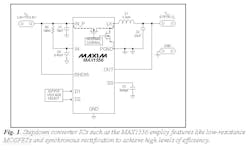
For curious souls, benchmark efficiencies can be obtained by examining the typical operating characteristics found in datasheets available from power-supply IC manufacturers. For example, the stepdown converter circuit in Fig. 1 achieves up to 97% efficiency for certain output configurations, and yields high efficiency for very light loads.
How are such high efficiency numbers realized? Paying careful attention to the fundamental losses common to all SMPSs is a great start. These losses are found largely in the switching components (MOSFETs and diodes) and, to a lesser extent, in the inductors and capacitors of the generic SMPS circuit. Depending on the IC, special features can be selected that will combat efficiency losses, such as control architecture options and component integration. For example, the circuit in Fig. 1 employs several methods to combat intrinsic losses including synchronous rectification, integrated low-resistance MOSFETs, low quiescent-current consumption, and a pulse-skipping control architecture, the benefits of which will be discussed as this article unfolds.
Brief Stepdown SMPS Overview
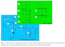
Although the losses that will be discussed are applicable to all basic SMPS topologies, the following text is explained with reference to the generic stepdown or buck converter circuit in Fig. 2. The figure also highlights some of the circuit’s switching waveforms that will be referred to in calculations presented later.
The stepdown converter reduces a higher dc-input voltage to a lower dc-output voltage. In doing so, a MOSFET is switched on and off at a constant modulation frequency (fS) by a pulse-width modulated (PWM) square wave signal. In a nutshell, when the MOSFET is on, the input supply charges the inductor and capacitor and delivers power to the load. During this time, the magnitude of the inductor current ramps up as it flows through Loop 1, as shown in Fig. 2.
When the MOSFET turns off, the input supply is disconnected from the output, and the inductor and output capacitor support the load. The magnitude of the inductor current ramps down as it flows through the diode, following the direction indicated in Loop 2. The fraction of the switching period in which the MOSFET is on is defined by the duty cycle (D) of the PWM signal. D divides each switching period (tS) into [D x tS] and [(1-D) x tS] intervals, which are associated with MOSFET conduction (Loop 1) and diode conduction (Loop 2), respectively.
All SMPS topologies use this division of the switching period to achieve output-voltage conversion. For the stepdown converter, the larger duty cycle is, the more energy is driven to the load, and average output voltage increases. Conversely, as duty cycle decreases, average output voltage decreases.
Due to this relationship, the conversion ratios for the stepdown SMPS are:
VOUT = D x VIN
IIN = D x IOUT.
It is important to note that the longer that any SMPS remains in a particular interval, the greater the relative losses are that coincide with that interval. For the stepdown converter, a low D signifies greater relative losses around Loop 2 since that loop dominates the switching period.
Switching Component Losses
The MOSFET and the diode depicted in Fig. 2 (and in most other basic converter topologies) tend to cause the largest degradation of efficiency due to the nature of these semiconductor devices. Both are victims of two varieties of power loss: conduction loss and switching loss.
The easier of the two to understand is conduction loss. Intuitively, where there is current flowing, there will naturally be an opposition to the current, and energy is expended as a result. Both the MOSFET and the diode act as switches that route current through the circuit when either device is on during each switching interval. Hence, a conduction loss will be generated when that particular device is on, due to the on-resistance of the MOSFET (RDSon) and the forward voltage of the diode.
Since MOSFET current flows only while it is on, MOSFET conduction loss (PCONDmosfet) is approximated by the product of RDSon, duty cycle and the square of on-state current:
PCONDmosfet = IMOSFETon(avg)2 x RDSon x D
where IMOSFETon(avg) is the average MOSFET current over the on-interval. Referring to the stepdown converter in Fig. 2, the MOSFET conducts output current (IOUT) while it is on, resulting in an estimated MOSFET conduction loss of:
PCONDmosfet = IOUT2 x RDSon x (VOUT / VIN)
While MOSFET conduction loss is proportional to the dissipation across its low RDSon, diode conduction loss is dependant on a comparatively larger forward voltage (VF). Thus, diodes usually have a larger conduction loss than MOSFETs. Diode conduction loss is proportional to forward current, VF and conduction time. Since the diode will conduct when the MOSFET is off, diode conduction loss (PCONDdiode) is approximated as:
PCONDdiode = IDIODEon(avg) x VF x (1-D)
where IDIODEon(avg) is the average diode current over the on-interval. In Fig. 2, average diode forward current is IOUT during its conduction interval. Therefore, PCONDdiode for a stepdown converter is estimated as:
PCONDdiode = IOUT x VF x (1 - VOUT / VIN)
By observing these equations, it is evident that the longer either device is on during each switching interval, the larger that device’s relative conduction loss. For a stepdown converter, the lower the output voltage is set (for a constant input voltage), the more the diode contributes to power loss, since it conducts for more of the switching interval.
Perhaps a bit less intuitive are MOSFET and diode switching losses, which arise due to the non-ideality of their switching characteristics. Time is required for the devices to transition from fully off to fully on, and vice versa, and that translates into power consumption as the devices change state.
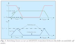
A simplified plot of drain-to-source voltage (VDS) and drain-to-source current (IDS) is usually given to explain the switching loss encountered in MOSFETs. The upper plot in Fig. 3 depicts such waveforms, where non-instantaneous voltage and current transitions occur during tSWon and tSWoff due to the charging and discharging of capacitances found in the MOSFET.
As indicated in the plots, full load current (ID) must be transferred to the MOSFET before its VDS decreases to its final on-state value (= ID x RDSon). Conversely, the turn-off transition demands that VDS increase to its final off-state value before current is transferred from the MOSFET. These transitions result in overlap of the voltage and current waveforms and lead to the power dissipation seen in the lower plot in Fig. 3.
Switching transition times are more or less constant over frequency, causing switching loss to increase as the frequency of the SMPS is raised. This can be understood by noting that the constant-transition periods consume more of the available switching period as that switching period shrinks.
A switching transition that requires only one-twentieth of the duty cycle will have much less of an effect on efficiency than one that consumes one-tenth of the duty cycle. Due to its frequency dependence, switching loss dominates conduction losses at high frequencies.
MOSFET switching loss (PSWmosfet) is estimated by applying triangular geometry to Fig. 3 to achieve following equation:
PSWmosfet0.5 x VD x ID x (tSWon + tSWoff) x fs
where VD is the drain-source voltage of the MOSFET during off-time, ID is the channel current during on-time, and tSWon and tSWoff are the turn-on and turn-off transition times, respectively. For the stepdown converter, VIN is applied across the MOSFET during the off-state, and it carries IOUT while it is on.
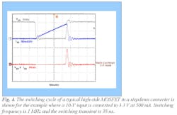
To demonstrate the aforementioned MOSFET conduction and switching loss equations, an oscilloscope was used to capture the VDS and IDS waveforms of a typical integrated high-side MOSFET in a stepdown converter. The conditions of the circuit were as follows: VIN = 10 V, VOUT = 3.3 V, IOUT = 500 mA, RDSon = 0.1 Ω, fS = 1 MHz, and the switching transient (tON + tOFF) is 38 ns.
As can be seen in Fig. 4, switching is not instantaneous, and the overlap in the current and voltage waveforms results in a power loss indicated by the lower waveform. The current waveform is ramped since IDS follows inductor current for the "on" cycle (Fig. 2), resulting in more switching loss occurring during the "off" transient.
Using the previously mentioned approximations, the total average MOSFET loss is calculated:
PTmosfet = PCONDmosfet + PSWmosfet
= IOUT2 x RDSon x (VOUT/VIN) + 0.5 x VIN x IOUT x (tSWon + tSWoff) x fs
= 0.52 x 0.1 x 0.33 + 0.5 x 10 x 0.5 x (38 x 10-9) x 1 x 106
PTmosfet = 103.3 mW
The result is consistent with the average value of 117.4 mW of the lower trace. Note that in this case, fS is high enough that PSWmosfet dominate conduction losses.
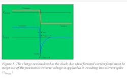
Like the MOSFET, the diode also exhibits switching loss. However, this loss depends to a large extent on the reverse-recovery time (tRR) of the diode used. Diode switching loss occurs during the transition of the diode from a forward- to reverse-biased condition.
Charge present in the diode due to forward current must be swept out of the junction as reverse voltage is applied to it, resulting in a current spike (IRRpeak) opposite of forward current. This action results in a V × I power loss, since reverse voltage is applied across the diode during this reverse-recovery event. Fig. 5 presents the simplified plot of a pn diode reverse-recovery period.
When the reverse-recovery characteristics of the diode are known, the following equation is used to estimate the switching power loss (PSWdiode) of the diode:
PSWdiodewhere VREVERSE is the reverse-bias voltage across the MOSFET, IRRpeak is the peak reverse-recovery current, tRR2 is that portion of the reverse-recovery time after IRR peaks. For the stepdown converter, VIN reverse-biases the diode after the MOSFET turns on.
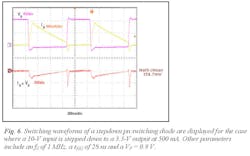
To demonstrate the diode equations, Fig. 6 displays the voltage and current waveforms observed for the pn switching diode in a typical stepdown converter. VIN = 10 V, VOUT = 3.3 V, measured IRRpeak = 250 mA, IOUT = 500 mA, fS = 1 MHz, tRR2 = 28 ns and VF = 0.9 V. Using these values:
PTOTALdiode = PSWdiode + PCONDdiode
= (1 - 0.33) x 0.5 x 0.9 + 0.5 x 10 x 0.25 x 28 x 10-9 x 1 x 106
= 301.5 mW + 35 mW
= 336.5 mW
This result coincides with the average power loss of 358.7 mW indicated in the lower plot in Fig. 6. Due to the large value of VF and the lengthy diode conduction interval, and since tRR is relatively fast, conduction losses (PSWdiode) dominate the diode.
Given the previous discussion, what can be done to mitigate the losses presented by the switching components of the power supply? The simple answer — choose MOSFETs with low RDSon and fast switching transients, and diodes with low VF and fast recovery periods.
Several phenomena directly affect the MOSFET on-state resistance. Naturally, RDSon increases with die dimensions and drain-source breakdown voltage (VBRdss), due to an increased amount of semiconductor material in the device. So, oversizing a MOSFET may introduce efficiency penalties that a smaller, properly chosen device might not have.
Further, due to the positive temperature coefficient of the MOSFET, RDSon increases as die temperature increases. Thus, proper thermal management practices must be followed to keep junction temperatures cool and ensure RDSon does not grow excessively.
The on-resistance also varies inversely with gate-source bias, up to a point. Therefore, a maximum gate-drive voltage is recommended to achieve lowest RDSon, with consideration given to the increased gate-drive loss introduced by doing so. However, gate-drive voltage is often not adjustable in SMPS ICs. That is, unless an option allows the user to do so, such as bootstrapping the IC supply, or when an external gate driver is used for an SMPS design.
MOSFET switching losses depend on the capacitances found in the device. Larger capacitances are slower to charge, causing switching transitions to last longer and to dissipate more power. Miller capacitance, commonly termed reverse transfer capacitance (CRSS) or gate-drain capacitance (CGD) in MOSFET data sheets, is a major contributor to transition times during switching.
The charge required by the Miller capacitance is denoted QGD, and as with the Miller capacitance, should be minimal for faster switching. Since MOSFET capacitance also varies with die size, a compromise between conduction and switching losses is usually considered, with careful attention given to the switching frequency of the circuit.
For the diode, forward voltage must be minimized, as losses due to it can be large. Forward voltage typically ranges between 0.7 V to 1.5 V for small, lower-rated diodes. Again, dimensions, process and voltage rating affect forward voltage and reverse-recovery time, with higher ratings and larger sizes exhibiting higher VF and tRR, resulting in greater loss.
Switching diodes geared toward high-speed applications are often categorized by speed, namely fast, super fast and ultrafast recovery diodes, with reverse-recovery time diminishing as speed increases. Fast diodes tend to have tRR in the hundreds of nanoseconds, while ultrafast diodes tend to be in the few tens of nanoseconds.
While pn diodes tend to have large forward-voltage drops, they are also available with large voltage and current ratings, making them suitable for higher-power applications. But, even with optimized VF and tRR diodes, one will not typically see a high-speed recovery diode in a low-power or portable application since the energy penalties are just too great.
As a possible alternative to fast recovery diodes in low-power applications, Schottky diodes offer virtually non-existent recovery times and VF that is nearly half that of fast recovery diodes (often from 0.4 V to 1 V), but are not available with voltage ratings as high as those of fast recovery diodes. Because of the benefits, Schottky diodes are widely used in low-power applications to greatly reduce the power loss associated with the switching diode, especially in low duty-cycle applications.
However, even with a low forward-voltage drop, the Schottky diode can present unacceptable conduction losses in low-voltage applications. Consider a stepdown output of 1.5 V, where a typical 0.5-V Schottky diode is used. This is 33% of the output voltage during the diode conduction time!
This high-loss situation can be improved by taking advantage of the low RDSon of a MOSFET in a technique called synchronous rectification. Here, a MOSFET replaces the diode (compare Fig. 1 and Fig 2) and is synchronized with the other MOSFET so that both conduct alternately during their respective switching intervals. Now, the relatively high VF of the diode is replaced by a much lower RDSon voltage drop (depending on current) of the MOSFET, recouping efficiency lost to diode conduction.
However, synchronous rectification does have its tradeoffs, such as increased complexity and cost, and it may not prove considerable benefit for very high-current levels, since conduction loss of the MOSFET increases as the square of its current. Additionally, since power is expended while turning on the gate of the synchronous rectifier, the engineer must weigh the efficient penalty of the additional gate drive.
The Data Sheet
This far, power losses intrinsic to the two major components of the generic switch-mode power supply, the MOSFET and diode, have been discussed. Recalling the stepdown circuit in Fig. 1, a few important aspects of the controller IC that aid in its very efficient operation can be related by referring to its data sheet.
First, the switching components are integrated into the IC package, thus saving space and reducing parasitic losses. Second, low RDSon MOSFETs are used. These are specified at 0.27 Ω (typical) and 0.19 Ω (typical) for the NMOS and PMOS, respectively. Third, synchronous rectification is employed. For a 50% duty cycle and 500-mA load, this reduces lower switch conduction loss from 250 mW if a 1-V diode were used, to approximately 34 mW due to the low RDSon of the synchronous NMOS transistor.
While switching components greatly influence SMPS efficiency, there are more areas where the engineer can combat the invasive effects of power loss. In the second part of this article, passive component losses and important efficiency enhancing features of SMPS ICs will be reviewed.
References
Mohan, Ned; Undeland, Tore M.; and Robbins, William P. Power Electronics: Converters, Applications, and Design, chapters 2, 7, 20 and 22, John Wiley & Sons, third edition, 2003.
This file type includes high-resolution graphics and schematics when applicable.


