ADI GaN Power Components and Tools Fuel Design Opportunities
Gallium nitride (GaN) semiconductors have come a long way since first becoming commercially viable as highly bright, blue light-emitting diodes (LEDs) in the early 1990s and, subsequently, a core technology for Blu-ray optical disk players. It would be almost two decades before the technology was commercially viable for field effect transistors (FETs) with high power efficiency.
GaN now represents one of the fastest-growing segments of the semiconductor industry, with compound annual growth estimates ranging from 25% to 50%, driven by demand for devices with greater energy efficiency to meet sustainability and electrification goals.
Sponsored Resources:
- Understand and apply supervisory ICS to avoid low-voltage power-up glitch headaches
- How to address DC/DC noise, efficiency, and layout issues using integrated power modules
- How to implement galvanic isolation for power and signal lines in high-voltage systems
GaN transistors can be used to design smaller, higher-efficiency devices than silicon transistors. Initially utilized for high-power microwave amplifier systems, the economies of scale in GaN fabrication and the ability to create small, more powerful amplifiers have expanded usage to create a multi-billion-dollar device market spanning consumer, industrial, and military applications.
Silicon MOSFETs are widely believed to have reached their theoretical limits for power electronics, while GaN FETs still have great potential for further performance advances. GaN semiconductors most commonly use silicon carbide (SiC) substrates, followed by silicon, which is more economical, or diamond, which is the best-performing and most expensive. GaN devices operate at higher temperatures with higher electron mobility and velocity than silicon-based devices and with low or zero reverse-recovery charge.
GaN power semiconductors feature about five times the power density of gallium arsenide (GaAs) power amplifier semiconductors. With a power efficiency of 80% or more, GaN semiconductors provide superior power, bandwidth, and efficiency over alternatives such as GaAs and laterally diffused metal-oxide semiconductors (LDMOS). The technology is now utilized in diverse applications ranging from fast-charge power adapters to light detection and ranging (LiDAR) devices incorporated into advanced driver assistance systems (ADAS) for automobiles.
Data centers represent another emerging market for GaN-based devices that can meet growing power consumption and cooling requirements for lower costs, as well as help address growing environmental disputes faced by operators in regulatory and political arenas.
Semiconductor manufacturers and market research firms also project a growing market for low- and high-voltage applications in electric vehicles, from more efficient batteries to battery traction inverters.
That's an area that has, to date, been dominated by SiC devices, which, like GaN, are classified as wide-bandgap (WBG) semiconductors with high electron mobility that "allow power electronic components to be smaller, faster, more reliable, and more efficient than their silicon (Si)-based counterparts." GaN has a bandgap of 3.4 eV, compared to 2.2 eV for SiC and 1.12 eV for SI.
GaN and SiC power semiconductors operate at higher frequencies and have faster switching speeds and lower conduction resistance than silicon. SiC devices can operate at higher voltages, while GaN devices provide faster switching with lower energy, allowing designers to reduce size and weight. SiC can support up to 1,200 volts, whereas GaN has generally been viewed as more appropriate for up to 650 volts, although higher voltage devices have been recently introduced.
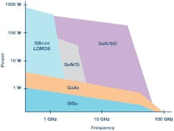
GaN can provide about 10 times the frequency range power compared to GaAs and other semiconductors (Figure 1).
Design considerations
It's estimated that 70% or more of electrical energy consumed worldwide is processed by power electronics. With the WBG characteristics of GaN, designers can create smaller power electronic systems, utilizing higher power density, superior efficiency, and ultra-fast switching speeds.
The technology enables innovation in multiple markets, including power electronics, automotive, solar energy storage, and data centers, among others. Highly resistant to radiation, GaN devices are well-suited to emerging military and aerospace applications.
Some electronic designers may have steered away from GaN power devices due to misperceptions regarding the cost of materials. While the fabrication of GaN substrate was initially much higher than Si, that differential has diminished considerably, and utilization of different substrates provides designers with the ability to find the best tradeoff between cost and performance.
GaN-on-SiC offers the broadest market potential for designers with the best tradeoff of cost and performance. However, with the options of GaN-on-Si and GaN-on-diamond, product designers can select the most appropriate substrate to meet the price/performance needs of their organizations and customers.
Due to the very high switching rates of GaN, designers need to pay particular attention to electromagnetic interference (EMI) and how it can be mitigated in the power-loop layout. Active gate drivers, which are essential for preventing voltage overshoot, can reduce EMI from switching waveforms.
Another key design issue is the parasitic inductance and capacitance that can result in false triggering. Maximizing performance advantages depends on the optimal layout of the lateral and vertical power loops and matching the speed of the driver to the speed of the device.
Designers also must optimize thermal management to prevent excessive heating that can compromise performance and reliability. Packaging should be evaluated on its ability to reduce inductances and dissipate heat.
Analog Devices sources GaN power amplifiers
Electronic systems require conversion between the voltage of the energy supply and the voltage of the circuitry that needs to be powered. Long-time leading semiconductor company Analog Devices, Inc. (ADI) aims to deliver industry-leading GaN power amplifier performance coupled with support, enabling designers to achieve top performance targets and get their solutions to market quicker.
Gate drivers and step-down (or buck) controllers are essential for maximizing the benefits of GaN power devices. Half-bridge GaN drivers enhance the switching performance and overall efficiency of power systems. DC-to-DC step-down converters convert a higher input voltage to a lower output voltage.
ADI offers the LT8418, a 100 V half-bridge GaN driver that integrates top and bottom driver stages, driver logic control, protections, and a bootstrap switch (Figure 2). It can be configured into synchronous half-bridge buck, or boost topologies. Split gate drivers adjust turn-on and turn-off slew rates of GaN FETs to optimize EMI performance.
ADI GaN driver inputs and outputs feature a default low-state to prevent false turn-on of GaN FETs. With a fast propagation delay of 10 ns, along with delay matching of 1.5 ns between the top and bottom channels, the LT8418 is suited for high-frequency DC/DC converters, motor drivers, class-D audio amplifiers, data center power supplies, and a broad range of power applications across consumer, industrial, and automotive markets.
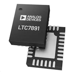
The LTC7890 and LTC7891 (Figure 3) are high performance, dual and single, respectively, step-down DC-to-DC switching regulator controllers for driving N-channel synchronous GaN FET power stages from input voltages up to 100 V. Aimed at addressing many of the challenges designers face using GaN FETs, these controllers simplify the application design by not requiring protection diodes or other additional external components typically used in silicon MOSFET solutions.
Each controller provides designers the ability to precisely adjust the gate driver voltage from 4 V to 5.5 V to optimize performance and allow the use of different GaN FETs and logic level MOSFETs. Internal smart bootstrap switches prevent overcharging of the BOOSTx pin to the SWx pin high-side driver supplies during dead times, protecting the gate of the top GaN FET.
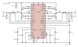
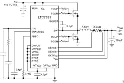
Both components internally optimize gate driver timing on both switching edges for near-zero dead times, improving efficiency, and allowing for high-frequency operation. Designers can also adjust dead times with external resistors. The devices are available with side wettable flanks in quad flat no-lead (QFN) packages. Schematics illustrate typical application circuits with the 40-lead, 6 mm x 6 mm LTC7890 (Figure 4) and the 28-lead, 4 mm x 5 mm LTC7891 (Figure 5) configurations.
Designers can also take advantage of a portfolio of ADI power management tools to achieve power supply performance goals and optimize boards. The toolset includes a variable buck resistor calculator, signal chain power configurator, and a Windows-based development environment.
Conclusion
GaN is a transformative semiconductor material used to produce components with high power density, ultra-fast switching speeds, and superior power efficiency. Product designers can leverage ADI’s GaN FET gate driver products to create more reliable and efficient systems with fewer components, resulting in smaller systems with reduced footprints and weight.


