Demystifying Deterministic Latency Within JESD204B Converters

For high-speed signal sampling and processing applications that need an array of synchronized analog-to-digital converters (ADCs), the ability to de-skew and match latency variation across the converters is paramount. System design around this feature is critical, as any latency mis-matches from the analog sample points to the processing blocks will degrade performance. Sample alignment also is needed for interleaved processing where one converter sample leads another by a fraction of a clock period.
Related Articles
- Prototyping Systems: JESD204B Converters And FPGAs
- Pair The Right JESD204B Converter With Your FPGA
- Synchronize Multiple ADCs With JESD204B
One of the key features of the JESD204B third-generation high-speed serial converter interface is its ability to establish a deterministic latency for each converter in the system. When this feature is understood and used correctly, it can create a synchronized or interleaved sampling system across many ADCs in a single system.
Since deterministic latency is a relatively new converter interface feature, system designers typically have several questions about how to establish it, the signals of interest, and how it can be implemented for synchronous or interleaved processing. Below are some common questions and answers for designing a system with deterministic latency used across multiple JESD204B converters that are sampled together with an FPGA.
This file type includes high resolution graphics and schematics when applicable.
What is deterministic latency, and how does JESD204B define it?
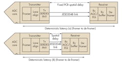
Deterministic latency across the JESD204B link is defined by the time it takes serial data to propagate from the parallel framed data input at the transmitter (ADC or source FPGA) to the parallel de-framed data output at the receiver (digital-to-analog converter, or DAC, or receiver FPGA). This time typically is measured in either frame clock periods of resolution or device clocks.
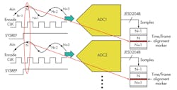
The JESD204B specification for deterministic latency does not consider the analog front-end core of an ADC or the back-end analog core of a DAC. It is only based on the data into and out of the JESD204B digital framing. Not only are two active devices a function in this latency computation, but also the spatial signal routing interfacing the two. This means the deterministic latency for each link could be larger or smaller within a multi-converter system, depending upon the spatial length of the JESD204B lane routing and their respective delays. Buffer delays on the receiver can help account for latency differences due to routing (Fig. 1).
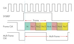
Unlike a simple serial link configuration, such as low-voltage differential signaling (LVDS), a JESD204B interface packs samples of data into defined frames. Each frame boundary of a couple or a few samples is marked by a special control character during the link handshaking, or initial lane alignment sequence (ILAS), from the transmitter. A larger defined group of frames, called a multi-frame, is also marked with a respective control character during the ILAS. However, after this sequence is complete, the control characters are not needed and the full bandwidth of the link can be garnered. Both the frame and multi-frame boundaries are coincident with a frame clock and multi-frame clock respectively.
What do JESD204B subclasses mean in relation to deterministic latency?
There are three subclasses of the JESD204B protocol to define the deterministic latency of the link. Subclass 0, which is backwards compatible with JESD204 and JESD204A, does not support deterministic latency. Subclass 1 supports deterministic latency by use of a system reference signal called SYSREF. Subclass 2 supports deterministic latency by a dual-purpose use of the ~SYNC signal, which also allows the receiver to initiate the handshaking ILAS routine. The ability to accurately place SYSREF versus ~SYNC in time relative to the clock will dictate which subclass is needed for the system of interest.
How can deterministic latency be used to align sampling across multiple converters?
For a subclass 1 converter implementation, frame clocks and multi-frame clocks are aligned internally on each device by the occurrence of the system reference edge, SYSREF. When a SYSREF edge is detected, both of these clocks are aligned to that point in time. Since these clocks remain internal to each device, their boundaries within the transmitters are communicated over the serial link by the use of control characters.
Each receiver can implicitly decode the placement of the transmitter frame and multi-frame clocks in time relative to its own clocks of the same name and relative to all transmit devices. This enables the receiver to de-skew the samples on the relatively early arrival of data to match the link with the latest arrival of data, using buffer delays (Fig. 2).
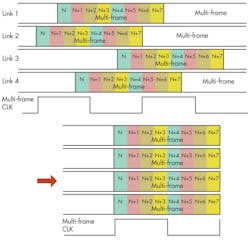
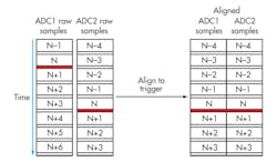
For synchronous sampling, these data links can be aligned in time within an FPGA. For interleaved sampling, each link can be offset by its corresponding relative phase delay. The deterministic latency can be identified for each link by measuring the delay in time from the receiver’s multi-frame clock edge until each respective link’s multi-frame control character. The caveat here is that the deterministic latency for each link must be shorter than the duration of a multi-frame clock period (Fig. 3).
Is deterministic latency the same as total converter latency?
The total latency of an ADC is the time it takes an analog sample to be clocked in, processed, and output digitally from the device. Similarly, the total latency of a DAC is the time from when the digital sample data is clocked into the part, until that corresponding sample is clocked out of the analog output. Typically, these are both measured in sample clock periods of resolution, as they are frequency dependent. It is partly a function of the analog processing architecture within the single converter component. This is fundamentally not the same definition as the deterministic latency described by a JESD204B link implementation, which is a function of three components.
What is the maximum de-skew budget for aligning multiple converters?
The transmitter sends multi-frame control characters to mark the multi-frame clock boundaries during the ILAS process. The receiver identifies these characters to create its own internal local multi-frame clock that is aligned with each of the transmitters in the upstream link. For large array systems where multiple receivers are used, the multi-frame clocks are also aligned across all of these devices. Therefore, the deterministic latency of any converter link cannot exceed the time of a single multi-frame clock period. This is the total de-skew time budget across the links.
The duration of a multi-frame clock is typically tens of sample clock cycles. It can even be adjusted longer or shorter through setup parameter variables that are communicated during the handshaking of the link.
Will this feature correctly align to the same analog sample point on either an ADC or a DAC, or is something more required?
Deterministic latency provides a way to align samples based on the same point in time as they are presented to the JESD204B framer. An ADC will have more clock periods of latency in addition to this time that are needed to process an analog sample from its front end ahead of the JESD204B framer. The converter vendor must specify this time period ahead of the framer in duration of clocks. Conversely, a DAC will need additional clock periods after the de-framer to process a sample to the output in analog form.
How long does the alignment process take before valid analog sample data is available?
A SYSREF edge sent to the converter and FPGA causes an alignment process to start. After this event, several multi-frame clock periods, in addition to the ILAS sequence, are required to complete before valid sample data is available. This is equivalent to a relative time of many sample clock periods. The specific duration may depend on unique deterministic delays of the JESD204B core in the converter and the value will need to be communicated by the vendor. During this time, the link will be brought down and valid data will not be transmitted. In absolute time, the duration will be a function of the sample clock frequency.
What is the most challenging system design aspect for achieving synchronous sampling?
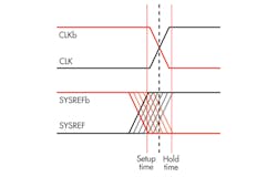
One of the most challenging aspects of achieving synchronous or interleaved processing down to the sample level in subclass 1 is the ability to align the enabling edge of SYSREF in time across multiple converters. In addition, each SYSREF edge will need to meet the setup and hold time to its respective sample clock. This will consume some of the available timing margin. The ability to actively and independently skew the fine phase between SYSREF and the clock will help achieve timing closure across the converters.
Does SYSREF need to be a single event or can it be recurring? What do I need to know about each case?
SYSREF alignment edges can be a one-shot pulse, periodic, gapped periodic, or recurring non-periodic. This will be dictated by the needs of the system and the timing flexibility of the phase skew between the clock and SYSREF at the source. For a recurring case of SYSREF, the frame and multi-frame clocks will be re-aligned on each event. However, since the goal is to maintain an aligned set of clocks, the enabling edge of a recurring periodic SYSREF should fall on multi-frame clock boundaries. Since the clocks should already be aligned after the first SYSREF edge, this will prevent unnecessary re-alignments.
One of the adverse effects of a periodic SYSREF signal is that there is the potential for it to couple onto the analog signal of interest. That’s why a periodic signal isn’t always recommended and should only be used if absolutely necessary. If a periodic SYSREF is used, care must be taken to properly isolate it from the analog front end of an ADC.
What are some ways that SYSREF skew can be adjusted to be within a single clock period?
Ideally, the SYSREF and clock for each converter and FPGA could be routed precisely, with timing margin to meet the strict setup and hold times across all components. But with the ever-increasing sample speeds of high-performance converters, timing closure cannot always be met with precise printed-circuit board (PCB) routing alone. Pin-to-pin variance across parts, coupled with supply and temperature drift, can create a relatively large timing skew across an array of high-speed converters. Advanced timing adjustment features may be needed to provide active SYSREF phase skew.
For example, an informative alert from an ADC could identify whether the SYSREF edge was latched within the setup and hold keep-out timing window. If this were to occur, ambiguity would exist for which clock edge is used for the timing reference, clock[N] or clock[N+1]. Depending upon where a SYSREF edge was detected, the phase of the sample CLK edge relative to SYSREF could be delayed at the clocking source to maintain a valid timing condition that meets setup and hold time.
Another option could be to use the next falling edge of the sample clock instead of the rising edge to get a half period of phase margin. Each converter in the system could be tuned this way, provided the clocking source has independent phase adjustment of the respective SYSREFs and CLKs (Fig. 4).
Is a converter with support of subclass 1 or subclass 2 required to use the deterministic latency feature?
Subclass 1 and subclass 2 are the only subclasses that support deterministic latency as described in the JESD204B specification. In subclass 1, the SYSREF signal defines the deterministic latency. In subclass 2, the ~SYNC is the signal that defines this latency. Some converter vendors, though, have created a subclass 0 implementation to be used for support of a synchronization scheme that aligns samples. In this case, the alignment procedure of the multi-frame clocks between converters and FPGAs is not used.
A time-stamping mechanism at the sample level could be used to mark the occurrence of SYSREF using appended auxiliary information known as control bits. Each sample that is coincident with a SYSREF edge is marked with a unique control bit. Within the FPGA, each link that has this timestamp can be delayed to equal the longest path and then aligned to each other, independent of the latency differences between the converters (Figures 5 and 6).
Summary
While deterministic latency is a somewhat complex option of JESD204B, when properly used, it can be a powerful feature for high-performance signal processing system design. Samples from an array of ADCs can be aligned and de-skewed within an FPGA by means of buffer delays to achieve synchronous or interleaved sampling. JESD204B subclass identification is important to understand the timing alignment capabilities of the system. Timing closure at the SYSREF and CLK input pins across the system ADCs is critical to achieving time aligned samples.
Ian Beavers is an applications engineer for the High Speed Converters team at Analog Devices Inc. He has worked for the company since 1999. Ian has over 18 years of experience in the semiconductor industry. He has a bachelor’s degree in electrical engineering from North Carolina State University and an MBA from the University of North Carolina at Greensboro. He is a member of EngineerZone’s High-Speed ADC Support Community. Feel free to send your questions to IanB on Analog Devices EngineerZone Online Technical Support Community.
About the Author
Ian Beavers
Product Engineering Manager, Automation Energy and Sensors, Analog Devices
Ian Beavers is a product engineering manager for the Automation Energy and Sensors Team located at Analog Devices, Greensboro, N.C. He has worked for the company since 1999. Ian has over 20 years of experience in the semiconductor industry. He earned a bachelor’s degree in electrical engineering from North Carolina State University and an M.B.A. from the University of North Carolina at Greensboro.
Comment About the Article
To join the conversation, and become an exclusive member of Electronic Design, create an account today!

Leaders relevant to this article: