Pair The Right JESD204B Converter With Your FPGA

With more analog-to-digital converters (ADCs) and digital-to-analog converters (DACs) now supporting the latest JESD204B serial interface standard, questions are arising about the best way to interface FPGAs to these analog counterparts. FPGA providers have been supporting multi-gigabit serialization/deserialization (SERDES) transceivers for many years now. In the past, though, most ADCs and DACs weren’t configured with these high-speed serial interfaces, meaning that FPGAs and converters did not interface with any common standard that took advantage of the high serializer-deserializer (SERDES) bandwidth.
Related Articles
- Slay Your System Dragons With JESD204B
- Kickstart Your System Designs With JESD204B
- Synchronize Multiple ADCs With JESD204B
The JESD204B interface was developed to address this gap by supporting the growing bandwidth needs of higher-speed converters. As a third-generation serial data link standard, JESD204B provides a higher maximum lane rate (up to 12.5 Gbits/s per channel), while supporting deterministic latency and harmonic frame clocking. This allows the interface to easily move large quantities of data for processing by taking advantage of higher-performance converters that are compatible and scalable with open-market FPGA solutions.
Most signal processing systems are first and foremost defined by their analog or RF frequency, dynamic range, and sample rate to establish the converter selection criteria. However, the converter’s digital interface considerations cannot be neglected when mating to an FPGA for data processing. Choosing the right JESD204B converter for your FPGA does not need to be difficult, by understanding the new JESD204B interface and keeping a few high-level considerations in mind. Below are some common questions and answers about mating JESD204B converters to an FPGA. They highlight the key concerns when designing in converters with this new serial interface.
What speed does my FPGA need to be for JESD204B?
Typically, the designer is really asking what transceiver line rate for the JESD204B interface to the converter the application FPGA needs to support. A transceiver is a high-speed serial interface within an FPGA that can send or receive data and recover an embedded clock. Transceivers are primarily high-speed data ports and functionally agnostic. But with the right firmware surrounding them, they can perform the digital support for many different interface protocols. An FPGA transceiver, for example, can serve as either a parallel to serial transmitter or a serial to parallel receiver (Fig. 1).
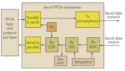
For a high-speed serial interface such as JESD204B, the FPGA transceiver can function in one of two ways in a system. When supporting the downstream capture of data out of an ADC, the FPGA will be the receiver of the serial data. As it receives data, the transceiver will convert the high-speed serial stream into parallel framed data for further downstream processing in the FPGA. Adaptive gain control (AGC), equalization (EQ), and clock/data recovery (CDR) are needed before converting the data from serial to parallel format.
When the FPGA is sourcing data to a DAC, it will perform the transmitter function. As a transmitter, it will frame the data and send it out serially on a high-speed interface. A pre-emphasis function, which will be discussed later, amplifies the signal for maximum transmission integrity.
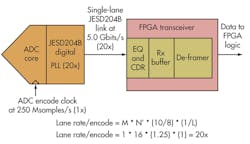
Typically the system’s analog sample rate or update rate will indirectly determine the FPGA’s transceiver line rate on the JESD204B interface. The converter’s clock, or encode rate, will have a phase-locked loop (PLL) multiplier factor to achieve the JESD204B bit rate. The maximum line rate supported by the converter may not necessarily be what your system requires, but should scale according to a known multiplier.
Figure 2 illustrates a single (M = 1) 16b (N’ = 16) ADC with a 250-Msample/s encode clock that can send data on a single JESD204B lane (L = 1) at a rate of 20 times (5 Gbits/s) the encode clock. The computation includes an 8b/10b encoding overhead. By using the converter at a different encode clock than 250 Msamples/s, the output lane rate will scale up or down with the same 20x multiplier.
What converter features can be used to lengthen the JESD204B link in a system and still maintain good data integrity?
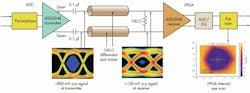
The JESD204B specification outlines criteria to meet a 20-cm transmission line. The printed-circuit board (PCB) material’s physical properties for the traces will play a dominant role in what attenuation the signal encounters during transmission. However, active channel compensation techniques on most converters and FPGAs help improve the performance of the link.
The converter or FPGA transmitter output can boost the high-bandwidth portion of the serial data while keeping the low-bandwidth portion unchanged. This technique is called pre-emphasis. Since low-pass signal attenuation will first affect the high-bandwidth portion of the signal (rise and fall times), pre-emphasis helps improve the transmission distance of the serial signal.
Similarly on the receiver, the DAC or FPGA can provide automatic gain control and EQ to the incoming signal to boost the high-frequency portion of the signal seen at the end of the transmission line. This technique usually has different gain and equalizer settings to help optimize the data recovery based on the system needs. Beyond the equalization stage, vendors such as Xilinx and Altera offer internal probing tools to visualize the data eye that is seen within the FPGA (Fig. 3).
What additional processing can be done on the converter to reduce the amount of data sent to or from the FPGA?
To reduce the computing burden on the FPGA, some converter vendors are adding digital processing as part of the total converter solution. Some signal processing systems only need to use a filtered portion of a signal bandwidth. Transmitting and processing full bandwidth data to or from the FPGA is only an overhead burden and not needed.
For example, an ADC can implement a digital down-conversion (DDC) function that effectively only sends the first of every four analog samples to the FPGA. Digitally filtering the data allows a lower data rate on the JESD204B interface and removes the need to have the DDC block on the FPGA.
Conversely, a DAC interpolation function may allow only one-quarter of the data rate to be sent from the FPGA to the DAC, with the other three out of four samples interpolated digitally with a complex algorithm. DAC interpolation methods permit only a subset of the data to be transmitted and then fully assembled within the converter before being output in analog form.
How many SERDES lanes per converter does my FPGA need to support?
The number of JESD204B lanes that interface from your converter to FPGA will be a function of line rate, converter sample rate, data packing efficiency, and whether your link uses single or multiple converters. While a converter may offer four JESD204B lanes, a system that runs at half of the maximum converter sample rate may only need to use two lanes. Each converter could implement the JESD204B lane count, speed, and data packing differently, based on the design. Check your converter datasheet to see what options are available that best fit the application.
Can I synchronize multiple converters to or from a single FPGA?
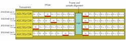
Yes, this can be done, provided that the FPGA supports enough lanes for the application needs. One of the key difficulties in a multi-ADC system is aligning sampled signals that have different latencies in time from analog to digital samples. The JESD204B interface has provisions for a system reference signal (SYSREF). This helps create a deterministic latency among the system converters that provides solutions for multiple converter synchronization. Since the data on the JESD204B is framed, the frames from multiple ADCs can be aligned in a post-processing step within the FPGA. This corrects for any latency mismatches between converters and FPGA transceivers.
Similarly, data to multiple DACs can be frame-aligned before it is sent from an FPGA. This allows for systems that require many converters to be synchronized through a single FPGA or just a few FPGAs. Some converter vendors also offer additional synchronization features that are outside of the formal specification to mark particular samples. If your system will require multiple converters to be synchronized, you will want to minimize the JESD204B lane count to and from the converters and choose an FPGA with maximum capability.
The JESD204B protocol has provisions to align sampled data from multiple ADCs with different latencies to be synchronized within the FPGA. Figure 4 shows how framed data or tagged samples from multiple links can be realigned for synchronous processing.
What FPGA fabric speed does my application need to process data?
The JESD204B interface uses an embedded clock to transport high-speed serial data. However, the FPGA will need a slower reference as the master clock to process the data. The FPGA family and model’s fabric speed will dictate this capability. It is important to consider what kind of processing your FPGA will be required to do with the converter data. For example, an application tasked with capturing periodic discrete data sets to memory compared to processing and moving out data continuously at full speed may require different FPGA fabric speeds.
How do I get JESD204B working on my FPGA?
A different way to phrase this request might be“Should I get the JESD204B firmware intellectual property (IP) from the FPGA manufacturer or develop it internally?” FPGA vendors such as Xilinx and Altera offer their own IP solutions for the JESD204, JESD204A, and JESD204B interfaces. These solutions can vary slightly depending upon the generation of JESD204 and the supporting FPGA model’s transceiver speeds.
Be sure to identify early in your converter selection process what form of FPGA and associated IP you will be using in your system. Your selection process should encompass the offerings of the FPGA vendor, the JESD204 generation being used, the FPGA family and model, and your internal technical code writing capabilities to implement the IP.
Some JESD204B converters may require a special additional application layer, or code “wrapper,” around the IP, which is essentially a unique set of firmware instructions. If this is the case, the converter vendor should identify this and be able to supply the application code to interface with the FPGA IP. The JESD204B converter should spell out in the datasheet what requirements are needed to support its link, though. Some converter manufacturers are also developing a battery of thorough validation testing between their devices and the FPGA firmware to prove out robustness.
Will my converter have a problem with an FPGA that has transceiver “frequency holes”?
Some FPGA models support transceivers that have gaps in their operation where known frequency ranges cannot be used. This can make the JESD204B lane frequency planning a bit more complex, but still manageable. Frequency planning for the converter sample rate and JESD204B lane rate are keys to staying out of the transceiver gaps.
Most converter systems typically have a fixed sample frequency. An occasional unique application needs to support just a few. Based on the fixed sample rate of the system converter and the JESD204B rate multiplier discussed earlier, a system designer can determine if the transceiver frequency gaps will cause a problem for the system.
Even if you find that the desired lane frequency falls right in the middle of a gap, read the converter datasheet to see if there could be some other options to tweak the lane rate. For example, it may be possible to change some of the other variables in the equation such as the lane count or the JESD204B sample resolution information to scale up or down the frequency curve and out of the transceiver frequency gap.
Summary
While the complexities of a new converter and FPGA interface like JESD204B can seem cumbersome, breaking down the key system needs is critical. Understanding the sample rate and JESD204B lane rate multiplier is essential. Planning and choosing the right FGPA model based on IP support, transceiver count, transceiver speed, and frequency gaps, if any, helps carve out the right choice for the converter. The selection of the right JESD204B converter can be simplified by focusing on just a few high-level criteria to mate with its FPGA.
This file type includes high resolution graphics and schematics when applicable.
Ian Beavers is an applications engineer for the High Speed Converters team at Analog Devices Inc., Greensboro, N.C. He has worked for the company since 1999 and has more than 15 years of experience in the semiconductor industry. He earned a bachelor’s degree in electrical engineering from North Carolina State University and an MBA from the University of North Carolina at Greensboro. He is a member of EngineerZone’s High-Speed ADC Support Community. Feel free to send your questions to IanB at the Analog Devices EngineerZone Online Technical Support Community.
About the Author
Ian Beavers
Product Engineering Manager, Automation Energy and Sensors, Analog Devices
Ian Beavers is a product engineering manager for the Automation Energy and Sensors Team located at Analog Devices, Greensboro, N.C. He has worked for the company since 1999. Ian has over 20 years of experience in the semiconductor industry. He earned a bachelor’s degree in electrical engineering from North Carolina State University and an M.B.A. from the University of North Carolina at Greensboro.
Comment About the Article
To join the conversation, and become an exclusive member of Electronic Design, create an account today!

Leaders relevant to this article: