Simplifying Device R&D and Basic System Test
The common thread connecting fundamental materials R&D and basic system test is the need to reduce time to insight. Having bigger displays and a kind of personal, real-time support engineer at your fingertips are two ways to help achieve that.
For anyone doing testing of any sort, having a methodical approach that tracks every change before each test run is critical. It’s common sense, of course, and engineers are taught this early on. Nevertheless, in R&D and at the early device characterization stage, a change in the output often occurs, and you may not be quite sure if it was caused by a device under test (DUT) or the test equipment. So you have to go back and check everything: the test rig, the probes, settings…even going back to test system recalibration.
This is a problem, especially at the fundamental materials and wafer level. The R&D team wants to focus on the R&D, not the test equipment, and especially not on whether the test equipment is giving the right results or not.
The sole focus on R&D to improve materials and processes for semiconductors is also increasingly being thwarted by the need to bring failure and reliability analysis, further up in the cycle, in parallel with materials and device R&D. This means doing failure analysis on the wafer instead of the package. The sooner a problem is identified, the better.
This is all a result of the insatiable need for faster, lower-power, higher-performance, more-reliable ICs for everything from communications and medical to automobiles and displays. Time-to-market competition is fierce, and no one wants field failures and the ensuing reputation fallout, not to mention the time spent taking the part back to the lab for analysis.
Let’s discuss two ways to simplify device test and characterization for device R&D teams: making it easier to see the test data and, at the same, simplifying the test set up itself (so that if unexpected data does occur, the team can focus on the device, and not the test rig).
Take transistor parametric analysis, for example, where both dc current-voltage (IV) and ac capacitance-voltage (CV) tests are required for each device. Switching back and forth and reconfiguring the cables can take hours, plus it introduces the potential for errors and doubt. At this stage of R&D, the users tend more toward being physicists, not experts in ground loops and impedance measurements.
One solution to the IV-CV test issue is to build two probe stations, which is a bit extreme (especially for smaller houses). Another option is to use a switch matrix, which can switch any input to any output. However, they tend to be large, and you usually don’t need all the output channels and the switching relays introduce losses.
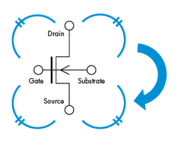
A better way may be to use an IV/CV multi-switch, like Tektronix’s new 4200A-CVIV. This is a small box that sits right in the middle between the DUT and the test equipment. This keeps the probe setup constant, minimizes the variables between tests, and literally lets you “walk around” the device terminals and do both dc and ac characterization without altering your setup (Fig. 1).
If there is an unexpected data reading, the 4200A-CVIV comes with an integrated display that shows clearly the probe positions (among other things), so they can be ruled out as a possible source of the error. If you want to add another device, the switch includes a pre-amp; pass-thru modules are also available.
Along with the 4200A-CVIV, Tektronix’s Keithley division also upgraded the first-gen 4200-SCS analyzer to the new 4200A-SCS, which features a bigger, high-definition display (15.9 in., 1920 × 1080) and your own personal support team. These come in the form of expert instructional videos embedded in the 4200-SCS to guide you through specific measurement procedures and projects.
The designers of the new 4200A-SCS also understood that the closer you get to a wafer’s surface, the more variable its topography, which can create measurement uncertainty. To accommodate for this, they built in optimization features to save time, including pin-to-pad contact confidence to ensure reliable measurements; C-V Confidence Check to confirm proper connections and measurements; and Pulse Preview to ensure correct pulse timing before testing begins.
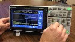
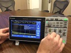
Tektronix applied the principles of big screens for more data display, as well as portable, personal tech support to its new generation of TBS2000 basic-level oscilloscopes (Fig. 2).
The TBS2000 line has a long history with students, professors and professionals alike, as well as the new generation of makers and maker-pros. The new TBS2000 has been upgraded through the addition of the 9-in. WVGA display with 15 horizontal divisions; the longest record length in its class, with 20 million points; on-the-fly, context-sensitive setting explanations; and an integrated handbook. With a long history in academia, the scope has been tightly coupled to Tektronix’s online courseware resource, which is updated regularly with new projects for educating students and professionals alike on how to perform specific tests. Again, it’s like having tech support at your fingertips.
Professors and teachers will appreciate the upgrade to Wi-Fi networking that’ll let them control, reset, and update all the scopes in a lab at once. It’s noteworthy that the new TBS2000 is also the only basic scope with the TekVPI Probe Interface that lets users access a wide range of Tektronix active probes. As the basic status indicates, it costs only $1,200, yet comes with a five-year warranty. Models are available with bandwidths of 70 MHz or 100 MHz and with two or four channels.
About the Author
Patrick Mannion Blog
Founder and Managing Director
Patrick Mannion is Founder and Managing Director of ClariTek, LLC, a high-tech editorial services company. After graduating with a National Diploma in Electronic Engineering from the Dundalk Institute of Technology, he worked for three years in the industry before starting a career in b2b media and events. He has been covering the engineering, technology, design, and the electronics industry for 25 years. His various roles included Components and Communications Editor at Electronic Design and more recently Brand Director for UBM's Electronics media, including EDN, EETimes, Embedded.com, and TechOnline.
Voice Your Opinion!
To join the conversation, and become an exclusive member of Electronic Design, create an account today!

Leaders relevant to this article:


