Use Photonics To Overcome The High-Speed Electronic Interconnect Bottleneck
This file type includes high resolution graphics and schematics when applicable.
“Addressing the electronic interconnect barrier through a technology like photonics is essential in keeping Moore’s law on track,” says Vernon Turner, senior vice president at IDC. In other words, electronic-based chip I/O is running out of steam, throttling bandwidth and acting as a bottleneck.
Copper-based chip-to-chip and board-to-board interconnects can’t support the high bit rates of stronger processing cores. Copper-based interconnects affect signal integrity, forcing design choices that compromise speed or distance. High speeds require smaller distances, so putting high-speed devices such as core routers on a rack and pooling their resources together, data center-style, as building blocks of a larger managed solution is not possible. It also limits device bandwidth. At high bit rates of 10 Gbits/s and higher, signal integrity becomes a key issue since the circuit ac characteristics begin to dominate the impedance, inductance, and conductance of the line, severely distorting the signal.
Related Articles
- Light-Speed Silicon-Photonic Devices Conquer "Big Data" Challenges
- Vibration Control System Simplifies Photonic Research
- Light Detection Technology Promises Highly Accurate Photon Counting
These effects are difficult to compensate for and can often result in serious attenuation at 10-Gbit/s data rates, requiring decision feedback equalization that may use upwards of 200 mW per 10-Gbit/s channel. For terabit scale links, up to 40 W could be consumed. As the practical limits of packaging technology such as printed-circuit board (PCB) material, cable design, and crosstalk of connectors are being reached, the possibility of designing switching systems at higher and higher speed rates becomes very expensive and impractical.
Electronics-based interconnects also force a compromise between I/O density and processing. Limiting bandwidth is not the only adverse effect of electronic interconnects, though. Devices that use electronics-based interconnects are power hungry, and many cases require cooling.
A Device-Based Point Of View
Let’s use a router to explain how chip-to-chip and board-to-board interconnects act as a bottleneck within a device. We can think of a router as a multi-processor system with a high-speed connection handling data transfer between processors. Traffic enters the router via one of the ports (ingress) and is routed to the processor that will carry out the various tasks of packet forwarding and buffering. Following these steps, the packet needs to be transferred to another ASIC in the system, and eventually it is transmitted to its destination through the designated exit port (egress). Data exchange between chips is a fundamental feature of the router. But at high bit rates the signal, sent over electronics, begins to deteriorate.
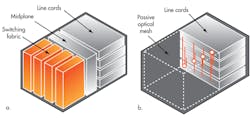
Traditionally, line cards are connected through a multi-layer midplane and switching fabric, where buffering and switching is done, creating numerous congestion points within the router (Fig. 1). We would argue that many of the midplane and switching fabric requirements stem from the bandwidth bottleneck. This results in a large system that is complex, requires significant power, and has limited bandwidth per slot.
Optics-Based Interconnect
A direct optical connection between processing elements such as the icPhotonics technology developed by Compass-EOS can overcome the interconnect problem described above. In this approach, photons are used for data transmission between chips. The electrical data is converted to an optical signal that can be routed via optical fibers from one point to the other.
There are numerous advantages to using photons instead of electrons for data transfer, including their low signal loss, minimal power requirement, high efficiency, and ability to transfer data over fibers with minimal loss. This technology overcomes a major bottleneck, and data can be exchanged efficiently between all chips in the system. When used for board-to-board connections, a full optical mesh can be designed.
An optical interconnect will convert the digital electronic signal into optical data and optical data into a digital signal, using a matrix of lasers and a matrix of photo detectors that are directly assembled on top of the CMOS chip. More precisely, digital data from the chip is converted to an analog data stream that directly modulates a laser transmitter. The opposite process, converting the received optical data into a digital signal, is carried out by coupling light from the fiber array to a matrix of photo detectors that convert the optical signal into an analog one that is then digitized.
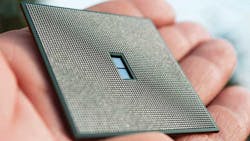
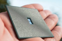
The CMOS chip upon which the optical interconnect is assembled is a custom designed ASIC that runs all of the logical tasks involved in data routing. The analog electronic circuits that drive the Tx and Rx channels are embedded in the center of the logic chip, yielding a hybrid device with digital and analog macros in a single, monolithic CMOS chip (Fig. 2).
Developing Silicon-To-Photonics Technology
Given the two optical chips and the analog macro embedded in the center of the CMOS chip, the first step in building the optical module is to assemble both chips on the CMOS. However, this is not a trivial task since there is a large difference in the coefficient values of thermal expansion between the laser and photodiode material (gallium arsenide and indium phosphide, respectively) and silicon. In such cases, optical chips can’t be bonded on silicon since the solder bumps fracture during the assembly process. A crack or delamination then forms in the solder material connecting both dies.
To overcome this problem, gold pillars were grown between the CMOS chips and the optical chips. Gold is the most malleable and ductile of all metals. Upon thermal change when both chips distort at different rates and direction, the gold pillar then deforms and will compensate for the unequal relative motion. Although this is not a novel idea, its application in large-scale matrices as used here is very difficult.
The process requires a complicated growth of the high-aspect-ratio gold pillars using electroplating techniques on the gallium-arsenide substrate. On the CMOS side, a copper pedestal is grown to allow connection of the gold pillar on the silicon. The bonding between the gold and copper bumps is carried out using a process known as eutectic bonding by mixing gold, copper, and a thin layer of tin. Upon melting the metals, a new intermetallic phase is formed that is responsible for the strength and durability of the optical module.
The next step is to optically couple the Tx and Rx channels to the fiber bundle in a manner that will allow data transfer between several ASICs in the system. The optical module is mounted onto the line card PCB, and two fiber bundle arrays are mounted on the PCB to facilitate optical interconnection and allow light coupling in and out of the device. The optical module has a hole in its center on both the PCB and substrate to provide access for fiber bundles to and out of the optical backplane.
The fibers used are multimode, 50/125-μm optical multimode 3 (OM3) fibers, suitable for 10-Gbit/s transmission up to 600 m. At the wavelength of operation (1000 nm), fiber loss is about 1 dB/km. Given typical fiber length in the system of about 2 m, the loss is negligible. For a multi-chassis configuration, fiber links of up to 200 m are supported by the designed optical link. The loss amounts to about 0.2 dB without any inter-symbol interference (ISI) on the signal.
The optical backplane simply comprises short (about 20 cm) 24 fiber jumper cables with appropriate optical backplane connectors that match those on the fiber bundle. There are seven slots of fiber jumpers in the backplane with 2×24 fibers in each since there is a Tx and Rx link for each backplane connection.
Impact On Device Design
The benefits of optics are not just the faster speed of chip-to-chip and board-to-board interconnects. They extend further, affecting the router itself, creating a higher-bandwidth router with a smaller footprint and lower power requirements.
Using a direct optical connection between processing elements makes the router midplane and central switching element unnecessary, as less buffering is required. A full mesh optical backplane replaces them and provides the required bandwidth for data exchange between chips and consequently radically reduces power consumption and footprint, packing a greener solution together with more bandwidth. In addition, with a fully passive optical backplane, the system’s airflow cooling is front to back, which is most efficient.
Where Silicon-To-Photonics Is Likely To Appear Next
Data exchange between ASICs is a core feature of many devices, from computing to the data center to sensing and medical devices. Although the Compass-EOS innovation was first implemented to create a novel kind of core router, the icPhotonics technology is applicable to similar challenges where interconnect barriers need to be broken to unleash the next wave of innovation.
In the data center and computing scenarios, icPhotonics can power high-density and low-power generic building blocks that can be used for a wide range of high-performance applications. Other I/O-challenged applications that are likely candidates for silicon-to-photonics evolution include high-performance computing, memory array systems, and storage array systems. It’s clear that photonics are here to stay, changing the landscape of electronic design.

About the Author
Asaf Somekh
Vice President of Marketing
Asaf Somekh joined Compass-EOS as vice president of marketing in 2012. Between 2001 and 2011, he served in several marketing executive positions at both Mellanox Technologies and Voltaire (acquired by Mellanox in 2011). Previously, he served as director of software R&D at Nexus Telocation and Aptel. He also held board member and group chair roles in industry associations such as the OpenFabrics Alliance and the InfiniBand Trade Association. He holds a BS in computer engineering from the Technion, Israel Institute of Technology, and an MBA from IMD in Lausanne, Switzerland. He can be reached at [email protected].
Comment About the Article
To join the conversation, and become an exclusive member of Electronic Design, create an account today!

Leaders relevant to this article: