Use Embedded Components To Improve PCB Performance And Reduce Size
The complexity and density of electronics design has increased, partly due to the rise of the mobile industry, introducing new challenges for printed-circuit board (PCB) designers. Embedding components within the board substrate offers a practical solution to several issues, and it’s quickly becoming a feasible production step for fabricators.
This file type includes high resolution graphics and schematics when applicapable.
Why Embed Components?
Before discussing the methods for adding embedded components to a design, it is important to understand some of the advantages they offer. One must consider all the benefits and drawbacks of adding fabrication steps before starting the design, in addition to the potential effects on cost and production yield.
Related Articles
- Passive Components Aren't Really So Passive (Part 3): PCBs
- Plan Ahead For Successful SoC-Based PCB Design
- The Engineer's Guide To High-Quality PCB Design
Reductions in size and cost drive innovation in PCB technology. Embedding components can help reduce the size of the board assembly. It also can potentially reduce the manufacturing cost for complex products.
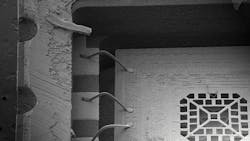
Minimizing electrical path lengths to reduce parasitic effects is critical when dealing with high-frequency circuits. Reducing the wiring length of passive components to an IC can decrease parasitic capacitance and inductance, reducing load fluctuations and noise within the system. By embedding passive components, it’s possible to position them directly underneath the pin of an IC, minimizing potential negative effects, including via inductance (Fig. 1).1
An integrated electromagnetic interference (EMI) shield can be manufactured directly around an embedded IC. Simply adding plated through-holes surrounding the IC can reduce capacitively and inductively coupled noise. It also can eliminate the need for an additional surface-mounted shield in certain applications.
Heat-conducting structures can be added to an embedded component easily, improving thermal management. One such example would be to embed thermal microvias in direct contact with an embedded component, allowing heat to dissipate to a thermal plane layer. Additionally, reducing the amount of PCB substrate that heat must travel through reduces thermal resistance.
Long-term reliability is a major source of difficulty and concern when implementing embedded components in a design. The sustainability of solder joints, when placed within the laminate framework of a PCB, is affected by subsequent soldering processes, such as reflow on surface-mount devices. Embedded components can cause additional problems after manufacturing, since they cannot be easily tested or replaced following a failure.
Types Of Embedded Components
Embedded components fall into two main categories, passive and active, but are largely used in different ways and for different purposes. Passives fill the large majority of components. Consequently, embedded capacitance and resistance has been studied comprehensively.
The term “embedded passive” does not generally refer to a discrete resistor or capacitor simply placed in a cavity within the board substrate. Rather, embedded passives are fabricated by choosing particular layer materials to form resistive or capacitive structures. While these types of embedded components were largely used at one point to save space, the development of smaller discrete passives (such as 01005 packages) have rendered them non-essential for that purpose in many designs.
Embedded passives still offer several benefits, including reduction of parasitic effects and size, and have become a common fabrication alternative to discrete surface-mount passives. This can be especially beneficial for applications such as series termination resistors, where hundreds of transmission lines enter dense ball-grid array (BGA) microprocessor and memory devices.
Manufacturing steps to place an IC within the board substrate can vary, but space must be created for the component body, in the form of a cavity. There are a few notable approaches to chip embedding technology:
• Integrated module board (IMB): Components are aligned and placed inside a cavity that is routed to the core laminate by controlled-depth routing. The cavity is filled with molding polymer to ensure chemical, mechanical, and electrical compatibility with the substrate. Isotropic solder is impregnated with the polymer to form reliable solder joints when the embedded part is laminated into the stack.
• Embedded wafer-level package (EWLP): All technology steps are performed at the wafer level. Fan-in is always required, meaning the area available for I/O is limited to the chip footprint size.
• Embedded chip buildup (ECBU): Chips are mounted to polyimide film, and interconnect structures are built up from there.
• Chip in polymer (CIP): Thin chips are embedded into buildup dielectric layers of PCBs, rather than integrating them into the core layers. Standard laminated substrate materials then can be used.
Considerations For Component Design
It’s important to consider the physical orientation and layout of components when designing for embedded purposes. Additionally, properly choosing compatible component and substrate materials helps reduce the chance of failure during manufacturing.
For embedded passives, choosing particular materials ultimately determines the electrical properties of those components. Embedded resistors are simply sheets of resistive film, dimensioned to achieve a certain resistance value. Resistance can be calculated using:

where ρ is the resistivity of the material, L is the length, and A is the area. (W and t are the width and thickness, respectively.) Resistivity varies for each resistive film material and is directly proportional to the final resistance value, meaning the material choice is a critical part of the design and manufacturing process.
Embedded capacitors are fabricated by arranging and dimensioning copper cladding as plates, with the dielectric material in between chosen accordingly. Capacitance can then be calculated using:

where εr is the dielectric constant of the material, ε0 is the permittivity of free space, A is the plate area, and d is the distance between the plates.
The dielectric constant varies based on the chosen material and is directly proportional to the final capacitance value. From this equation it is clear that capacitance is increased by decreasing plane-to-plane distance in the board layers and by maximizing the plane areas. Special materials are available that allow dielectric strength to be maintained while producing a dimensionally stable, yet very thin, plane-to-plane dielectric layer to increase plane capacitance for power supply decoupling.
For embedded ICs and other active components, materials are chosen primarily to account for long-term reliability of components in cavities and for substrate durability. Coefficient of thermal expansion (CTE) can describe how a material will change and react to high-temperature events or processes, such as reflow soldering performed for surface-mount components. If CTE (specifically z-axis expansion) is mismatched between the substrate material and polymer used to fill cavities, the board structure and integrity can be compromised.
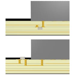
Two basic process flows are used when aligning and placing embedded passive and active components in cavities: face-up and face-down. By embedding components face-down, it is only required that cavities be created at a depth equal to the package height, meaning several chips of different thicknesses can be embedded on the same layer. Face-down manufacturing allows for good dielectric material thickness control, as well as good component placement accuracy during the assembly process.
Manufacturing Process
Manufacturing steps will vary based on the process decided by each individual fabricator, as well as the available equipment for manufacturing. Generally, the manufacturing process for embedding components can be split into two categories: components aligned and placed within cavities, and components molded into the substrate, with additional structures built up from there.
PCB cavities can be formed using different configurations and manufacturing techniques. As the technology for embedding active components has advanced, newer and more efficient methods for developing cavities have been developed, with improved reliability and higher production yield as added benefits.
Laser drilling cavities offers the highest precision and positional accuracy of any method. The laser beam is precisely controlled to achieve uniform depth control and wear, as dielectric material is removed. Since the laser typically uses a large wavelength, it cannot penetrate copper layers, establishing a well-defined “stop layer” for the process. After the cavity has been formed, an anisotropic conductive adhesive substance is added, and a component is placed in the void. Heat is applied to the system at a specific pressure to melt the solder particles dispersed in the adhesive material and form reliable solder bonds.
Milling offers a more conventional and cost-effective approach for creating cavities. Milling tools have been reduced in size enough to keep up with most modern fabrication needs, but there is a practical limit to the processing technology. Nevertheless, milling and routing technology is better established than laser drilling, so it is more readily available for creating cavities.
Thin wafer packages can be integrated directly into buildup dielectric layers, rather than utilizing cavities drilled or routed into core material. Standard laminated substrate materials such as multilayer FR-4 then can be used, reducing cost and risk to production yield. First, a thin chip is die-bonded to a substrate. Next, either a liquid epoxy or a laminated resin-coated copper (RCC) film is applied as dielectric. By optimizing the heated press lamination process, the chip can be embedded without voids.
Recommended Documentation
Properly documenting a design with embedded components can go a long way toward reducing manufacturing time and cost. The embedded components process combines PCB manufacturing, component packaging, and component assembly into a single manufacturing process flow:
• Layer stack diagram: A cursory diagram shows the location and orientation of cavities for embedded components.
• NC drill file: A separate file should be generated to account for cavities. This information is much more detailed and accurate than a layer stack diagram, and it will be used during bare-board fabrication for routing or punching.
• Fabrication notes: Any useful information for the fabrication process should be noted. This may include specific substrate material choices or polymer and epoxy materials used to fill cavities.
• Pick-and-place file: A separate file should be generated for components to be embedded. It should include information about component location, rotation, and layer.
• Assembly notes: Additional assembly information not included in the pick-and-place file should be noted. This may include whether the component is flipped on the layer or any special assembly instructions.
Examples Of Embedded Components
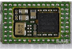
With increasingly more efficient manufacturing processes being developed, devices utilizing embedding components have become more prevalent. Wireless modules often are employed to reduce a board’s profile (Fig. 2).
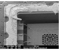
A die also can be placed in a cavity (Fig. 3).
Stacked die can be used within a chip as well (Fig. 4).

This eliminates the need to put it into a cavity, but stacked-die chips are more expensive.
Conclusion
Although the technology for embedding passive and active components within the board substrate has been available for some time, it has only recently become commercially viable to perform such steps during manufacturing. Market demand for high-density, low-profile electronic devices has pushed past the potential drawbacks, such as reliability concerns and risks to cost and production yield.
This file type includes high resolution graphics and schematics when applicapable.
References
1. Palm, P., Moisala, J., Kivikero, A., Tuominen, R., & Iihola, A. (2005, March). Embedding active components inside printed circuit board (PCB)-a solution for miniaturization of electronics. In Advanced Packaging Materials: Processes, Properties and Interfaces, 2005. Proceedings. International Symposium on (pp. 1-4). IEEE.
2. Tuominen, R. Embedded Components in PCB [PDF document]. Retrieved November 18, 2013, from: http://www.powersoc.org/PwrSOC08/Presentations/Received/Invited%20Talk%20S6x7%20-%20Risto%20Tuominen%20-%20Embedded%20Components%20in%20PCB.pdf.
3. Brunnbauer, M., Furgut, E., Beer, G., Meyer, T., Hedler, H., Belonio, J., ... & Kobayashi, K. (2006, May). An embedded device technology based on a molded reconfigured wafer. In Electronic Components and Technology Conference, 2006. Proceedings. 56th (pp. 5-pp). IEEE.
4. Maia Filho, W.C., Brizoux, M., & Grivon, A. (2010, April). Optimization of PCB build-up layer configuration for electronic assemblies with active embedded components in the board. In Thermal, Mechanical & Multi-Physics Simulation, and Experiments in Microelectronics and Microsystems (EuroSimE), 2010 11th International Conference on (pp. 1-5). IEEE.
5. Schönholz, R. (2009). Embedded Active Devices. Circuit Board Technology, 5, 1-4. Retrieved November 18, 2013, from: http://www.we-online.com/web/en/leiterplatten/produkte_/embedding/lasercavity_1/veroeffentlichungen_1/Tec_Report.php.
6. Aschenbrenner, R., Ostmann, A., Neumann, A., & Reichl, H. (2004, December). Process flow and manufacturing concept for embedded active devices. In Electronics Packaging Technology Conference, 2004. EPTC 2004. Proceedings of 6th (pp. 605-609). IEEE.
7. SKY85303-11 Package Bottom [Photograph]. (2013). Retrieved November 18, 2013, from: http://www.chipworks.com/en/technical-competitive-analysis/resources/blog/inside-the-samsung-galaxy-s4/
8. MEMSIC MXD6125Q thermal accelerometer [Photograph]. (2010). Retrieved November 18, 2013, from: http://www.chipworks.com/en/technical-competitive-analysis/resources/blog/mems-by-the-sea-itll-be-a-rough-trip/
9. Laminated stack of 4 dummy UTCPs [Photograph]. (2009). Retrieved November 18, 2013, from: http://www.imec.be/ScientificReport/SR2009/HTML/1213550.html

About the Author
Max Clemons
Application Engineer
Max Clemons is an application engineer at Altium focused on developing electronic design content. He is an IPC Certified Interconnect Designer, with experience researching electronic materials and green energy devices. He received his BSEE from the University of California, San Diego. He can be reached at [email protected].
Comment About the Article
To join the conversation, and become an exclusive member of Electronic Design, create an account today!

Leaders relevant to this article: