This file type includes high resolution graphics and schematics when applicable.
For many, a good rule of thumb for switch-mode power designs has been that hard switching is easy, and soft switching is hard. Power-switching technology developments, however, give reason to switch thumbs.
Key specifications for most power-conversion implementations include cost, power density, efficiency, transient response, output ripple, electromagnetic interference (EMI) emissions, and total design-in time. Hard-switched power converters have the advantage of being relatively quick and easy to implement. Additionally, their control structures are small and simple so, if all other things were equal, they are comparatively inexpensive as well. However, all other things aren’t equal, so a more careful comparison is necessary to evaluate the relative merits of hard-switched and soft-switched power trains.
Related Articles
- 7 Critical Steps In Switching Power Supply Design
- Choosing The Right Switching Regulator
- Switch-Mode ICs Promote Efficient Power Management
Conversion losses limit power density and efficiency. Switching losses also limit operating frequency. Dominant switching-loss terms are attributable to the turn-on behavior of a power train’s high-side MOSFET and the Miller gate charge.1 Switching losses increase with, and thus limit, switching frequency. Body-diode conduction losses detract further from power-conversion efficiency in hard-switched converters.
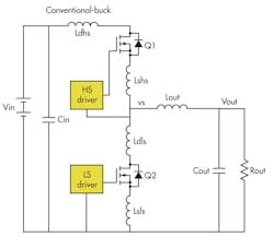
In a synchronous buck topology, the high-side FET turns on when it has the maximum voltage across it in hard-switched converters (Fig. 1). It conducts its maximum current during the turn-on portion of the operating cycle. Power losses in the high-side switch, therefore, are at a maximum during the off-on transition. The larger the input voltage, the higher the power loss, so converters in high voltage-ratio applications (e.g., 24 V to 3.3 V) tend to deliver poorer efficiency than the same converters in circuits demanding lower conversion ratios (e.g., 5 V to 2.5 V).
The alternative, soft switching, significantly reduces these switching losses. Soft switching techniques require more complex control circuits because the switch timing must be coordinated with the switched waveform.
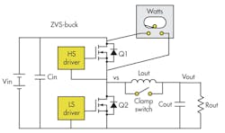
One example of soft switching is the ZVS (zero-voltage switching) technique, which improves conversion efficiency across a range of power topologies. As the name suggests, ZVS switches the high-side FET on when the voltage across the switch is at or near zero (Fig. 2). This breaks the link between power losses and the voltage conversion ratio during the high-side FET’s turn-on interval.
Operation of a clamp switch with the ZVS technique allows the converter to store a small amount of energy in the output inductor when both high-side and low-side switches are off. The converter uses this energy to discharge the high-side FET’s output capacitance and charge synch FET’s output parasitic.
Taking the FET’s output capacitance out of the switch’s turn-on behavior desensitizes FET selection with regard to CGD and, consequently, allows designers to focus on on-state channel resistance instead of traditional figures of merit such as the product of channel resistance and gate capacitance.
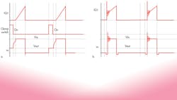
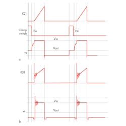
This method of driving the high-side FET during turn-on avoids exciting the switch’s parasitic inductance and capacitance, which tend to resonate, inducing large voltage spikes and ringing in hard-switched topologies (Fig. 3). By eliminating the spikes and preventing the ringing, ZVS removes another power-loss term and eliminates a source of EMI emission.
Eliminating the voltage spikes from the switching behavior also allows designers to select lower-voltage FETs with lower RDS(ON). One lasting rule of thumb (first-order approximation) is that for a given FET technology and die size, the RDS(ON)s of two FETs with different VDS(BR) will compare as:
A lower-voltage FET further improves efficiency by reducing conduction losses through the switch. So, for example, replacing a 30-V power MOSFET with a 20-V device can reduce the RDS(ON) and so I2R loss by a factor of about 2.7.
By arranging the high-side FET to turn on with low switching loss, the converter can switch at substantially higher frequencies than hard-switched converters. For example, many of Vicor’s soft-switched products operate at 1.5 MHz or more—two to three times faster than hard-switched high-density converters.
The increase in switching rate enables OEMs to deploy soft-switched power conversion devices with smaller output-filter components, saving both board space and component costs. The faster switching rate also permits many soft-switched converters to respond more quickly to load transients.
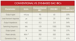
Soft switching is extremely versatile. For example, Vicor uses the technique in its VI Chip and VI Brick products where it provides key benefits to its SAC (Sine Amplitude Converter) topology among others. In intermediate bus converter (IBC) applications, the ZVS-based SAC topology delivers noteworthy performance improvements in as many as seven performance parameters (see the table).
Design-in is as easy as hard-switched power-conversion components, and the soft-switched devices provide notable improvements in conversion efficiency, power density, EMI, and output ripple. They currently serve in power subsystems with ac, HVDC (380 V), 48-V, and 12-V inputs, with and without isolation, and at power levels from 15 to 1200 W.
Reference
“The PI33xx: Zero-voltage switching applied to buck regulation,” white paper, Vicor, July 2012.
Stephen Oliver is vice president of the VI Chip product line for Vicor Corp. He has been in the electronics industry for 18 years, with experience as an applications engineer and in product development, manufacturing, and strategic product marketing in the ac-dc, telecom, defense, processor power, and automotive markets. Previously, he worked for International Rectifier, Philips Electronics, and Motorola. He holds a BSEE from Manchester University, U.K., and an MBA in global strategy and marketing from UCLA. He holds several power-electronics patents as well.
About the Author
Stephen Oliver
Vicor Corp., Power Design
Stephen Oliver, vice president of Vicor’s VI Chip Product Line, has been in the electronics industry for 18 years, with experience in applications engineering, product development, manufacturing, and strategic product marketing in the ac-dc, telecom, defense, processor power, and automotive markets. Previously with International Rectifier, Philips Electronics, and Motorola, he received a BSEE degree from Manchester University, the U.K., and an MBA in global strategy and marketing from UCLA. He holds several power electronics patents as well.
