Design for manufacturing (DFM) as a concept seems both self-explanatory and obvious. After all, in a corporate context, the entire point of designing something is to manufacture and sell it. Because the designer’s primary intent is to address features demanded by the market, it can be useful to add a specific design focus on manufacturing. Indeed, DFM practices and tools are pervasive across a wide variety of industries impacting products as diverse as cars1 and torpedoes.2
Related Articles
• Taking DFM To The Heart Of The Design Flow
• Design Flows Must Evolve Toward DFM Awareness
In the semiconductor industry, the term DFM has been applied to a wide variety of initiatives and applications including critical area analysis, lithographic printability, redundant via algorithms, wire spreading, and more. Simply put, DFM can best be described as efforts made to optimize a design for highest manufacturing yield given known manufacturing limitations. Historically, the oldest and most ubiquitous DFM tool in the semiconductor industry has been the design rule manual (DRM).
Increasing Design Rule Complexity
A modern DRM lists what is and isn’t allowed from a physical design perspective. Often, the DRM document really focuses on listing what isn’t allowed. As the complexity of the semiconductor processes (particularly sub-wavelength lithography) has grown, so too has the list of disallowed design shapes and, by extension, the complexity of the DRM itself. Over the last two decades, DRMs have grown exponentially.3
This increasing DRM complexity can be explained in part by the difficulty that rule-based polygon design rule checkers have with capturing sophisticated physical effects, such as lithography effects. Ten years ago it was sufficient to specify a minimum allowed space that a designer could draw based on the available lithographic capability.
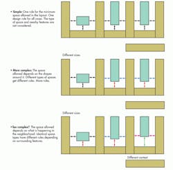
Today, the minimum space that can be manufactured depends on the exact layout (e.g., run length of the space) and the proximity of the space to other geometries (Fig. 1). Since every layout is potentially different, there are many cases for a rule writer to consider. The need to specify all the allowed, special, and forbidden cases is a primary reason for the modern DRM’s increasing girth.
1. Not all spaces are created equal. The ability to print a design space during manufacturing can depend on the type of space being printed and on other geometries nearby.
The Need For Models
The increasing pressure on design rules is completely analogous to events in the optical proximity correction (OPC) area 10 years ago. As lithographic rules for correcting diffraction effects in manufacturing steppers became too complex to manage in a rule-based table, lithographers turned to model-based OPC. The advantage of model-based OPC is that each polygon can be considered individually, based on its shape and the impact of surrounding geometries unique to that particular design.
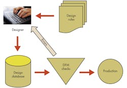
In a like manner, manufacturing teams began to understand that two-dimensional rule checking would not be sufficient to capture the increasing number of complex interactions efficiently. In response, model-based DFM tools were developed. Flows allowing designers to run “DFM checks” prior to committing their design to production were implemented (Fig. 2).
2. During design in a typical DFM flow, layouts are checked for manufacturability and errors are fed back to designers for disposition.
Similar to historical design rule checks (DRCs), sophisticated simulations would “pass” or “fail” the designs based on physical simulations that considered manufacturing effects and design requirements simultaneously. Any problem areas or “hotspots” identified would be marked as failing and passed back to the designer.
Challenges With Existing DFM Flows
Indeed, such DFM flows have been implemented in the industry in practice.4 But DFM flows at advanced CMOS nodes have faced the following challenges that threaten widespread adoption:
• Model availability: In general, DFM tools require models. As discussed previously, one of the real challenges of delivering design kits on time is model accuracy.5 Typically, at the beginning of a CMOS node when time-to-market is critical, model coverage and accuracy are limited. This hampers the effectiveness of DFM tools delivered in the design kits.
• Competition with restricted design rules: One alternative to DFM tools is implementation of restrictive design rules.6 The more restrictive the design rules, the fewer the special cases that will need to be considered. At some point, there will be so few cases to consider that traditional design rules will suffice. A case in point is fixed-pitch poly gate layers where field poly turns are not allowed. With the pitch fixed, all that remains is a simple grating without the need for sophisticated DFM tool analysis.
• Continuous improvement: As semiconductor processes mature, they generally increase in stability and predictability with increasing margin. When hotspots are identified, process engineers naturally try to improve their processes. A mature process with “fixes” and well-known limitations has less need for DFM analysis than a new process with lots of problems and surprises. Indeed, we have seen several cases where DFM flows have been “turned off” in mature processes because the flows were no longer detecting hotspots.
• Design cycle time: One common complaint from designers is that the results of DFM analysis often come too late in the design flow. A great example of this is chemical mechanical polish (CMP) simulation, where analysis can only be run after large layout blocks have been assembled. CMP is a macroscopic process and requires a large area simulation. Once the layout is at the stage where CMP can be run, “fixing” DFM errors can be very costly in terms of design cycle time, which ultimately affects time-to-market.
• Cost: Of course, model-based simulations can be computationally expensive to run, both in terms of time and real cost (computer hardware and software license cost). In an era where large system design budgets can be on the order of $100 million, cost is a concern.
DFM As An Engineering Tool
Rather than the wholesale adoption of DFM as a design flow requirement for all current and future technology nodes, a more likely path for DFM tool use lies in engineering. During technology development prior to ramp, DFM flows can be very useful in identifying inherent problems by studying early layouts.
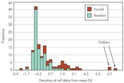
DFM tools have been successfully utilized to study layouts to identify “problem cells” in early design libraries.7 Once identified, the problem cells are fixed and further DFM study of the “DFM certified” cell library is no longer required (Fig. 3).
3. DFM tools can be used to analyze entire cell libraries. By simulating manufacturing variation in both “forced” and “random” design test cases, “bad cells” are identified and fixed for all future designs, eliminating the need for future checks of those cells.
This use of DFM tools for engineering study leverages their power while avoiding many of the cycle time, cost, and accuracy concerns that full design deployment can raise. For this reason, the future of DFM tools seems important, but different than what was originally envisioned.
Sources
1. Laura Carrabine, April 19, 2010, “Ford Drives Assembly Innovation,” DesignWorld, www.designworldonline.com/ford-drives-assembly-innovation/
2. Barber-Nichols Inc., 2011, “Design For Manufacturability,” Barber-Nichols, www.barber-nichols.com/case-studies/design-manufacturability
3. Ed Sperling, December 13, 2012, “Too Many Rules,” Semiconductor Manufacturing and Design, http://semimd.com/blog/2012/12/13/too-many-rules/
4. Philippe Hurat, Jianhao Zhu, and Edward Teoh, 2012, “Electrical design for manufacturability and lithography and stress variability hotspot detection flows at 28nmn,” Proc. SPIE 8327, http://dx.doi.org/10.1117/12.916742
5. Mason, M.E., 2012, Design enablement: The challenge of being early, accurate, and complete," VLSI Technology (VLSIT), 2012 Symposium, 10.1109/VLSIT.2012.624503, pages 145-146
7. Kayvan Sadra, Mark Terry, Arjun Rajagopal, Robert A. Soper, Donald Kolarik, Tom Aton, Brian Hornung, Rajesh Khamankar, Philippe Hurat, Bala Kasthuri, Yajun Ran, and Nishath Verghese, 2009, “Variations in timing and leakage power of 45nm library cells due to lithography and stress effects,” Proc. SPIE. 7275, Design for Manufacturability through Design-Process Integration III 72750K. doi: 10.1117/12.816485


