Achieve High Power Density with Stacked Inductors
This article is part of the Power Management Series: Delving Into Power Density
Members can download this article in PDF format.
What you'll learn:
- Using magnetic resonance in wireless power transfer tech.
- A stacked buck-capacitor methodology.
- The 3D multi-spiral inductor design.
- Designing and implementing an air-core embedded inductor onto a PCB.
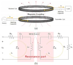
One method involved in wireless power transfer (WPT) technology is to employ magnetic resonance with tight magnetic coupling. Researchers have measured a resonance in vertical multi-coupled coils that have tight magnetic coupling. They also analyzed the transferred power with respect to resonances of vertical multi-coupled coils.
Tests have been validated and determined that both series and parallel resonant frequencies of input impedance coincide with the frequency at which the transferred power is increased. It’s also been validated that the series resonant frequencies of the input impedance coincide with the frequencies at which the EMI has increased for a constant ac voltage source (Fig. 1).
Because impedance matching is employed, a resonant peak is generated at the input impedance of each coil. The frequency of this peak is utilized for the power transfer frequency.
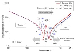
However, if a design chooses tight magnetic coupling, the resonant peak of the input impedance is divided into several peaks due to the increase of mutual inductance between coupled coils. In this case, the frequencies of maximum transferred power are changed (Fig. 2).
In this example, there will be changes in input impedance as the number of the vertical multi-coupled coils is increased to #N (the number of coils). As the number of the vertical multi-coupled coils is increased to #N, the number of the series resonance peaks also will increase to #N and parallel resonance peaks to #(N-1). The total number of resonance peaks changes to #(2N-1). The distance between resonances widens farther and farther as the mutual inductance increases, due to the addition of more coils.
Benefits of Stacked vs. Side-by-Side Coils
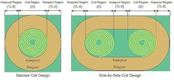
Stacked coils hold an advantage over side-by-side coils because they have a smaller footprint on the PCB. Designers need to be careful not to route components too close to the sensing coils in order to achieve the optimum sensitivity and channel-to-channel match. This means better power density.
“Keepout” distance is recommended to at least half the coil diameter from the sensors. In a side-by-side arrangement, the minimum PCB area for routing the sensor is 2 coil diameters high and 3.5 coil diameters wide. The stacked arrangement only needs 2 coil diameters high and wide (Fig. 3).
Passive-Stacked Buck Converter Achieves High Power Density
In a conventional buck dc-dc converter, small inductances will help achieve high power density. However, these small inductors will have a high dc resistance (DCR), so they will limit the achievable power density of a small buck converter to less than 0.4 W/mm2.
Recent efforts in using switched-capacitor (SC) networks can lead to improved power density. The caveat is that to achieve this, designers will need to use fairly exotic ultra-high-density capacitors that can operate over a small number of conversion ratios. When increasing the number of ratios to help achieve good dynamic voltage scaling (DVS), loads like 0.4 to 1.2 V along with conventional capacitors will lower power density to much less than 0.1 W/mm2.
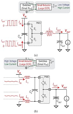
To improve power density in these instances, a hybrid dc-dc converter topology can split the inductor, from a conventional buck converter, into two half-sized inductors that can be stacked on top of and below the input coupling capacitor. That input coupling capacitor is then “flying” and forms a passive-stacked third-order buck (PS3B) converter.
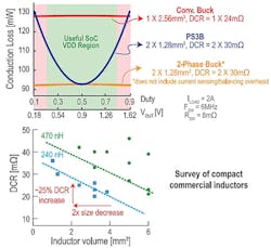
This design architecture isn’t like a conventional buck converter whereby its small inductor, which will have a larger DCR than the switches in a well-designed, comparably sized power-management integrated circuit (PMIC), processes power on the high-current/low-voltage side of the converter. The stacked inductors in the PS3B process power on the low-current/high-voltage side of the converter. Even when designers account for the larger DCR imposed by the half-sized inductors, the overall conduction loss of the PS3B converter is up to 1.4X lower than an equivalent-area conventional buck converter.
The input current in the PS3B also is continuous, as opposed to the fully pulsated input current of a conventional buck converter, which will help reduce the area of the passives required for filtering. This design has an increased power density over the previous design mentioned above when including the area of passives (Figs. 4 and 5).
3D Multi-Spiral Inductor
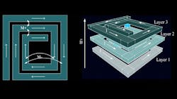
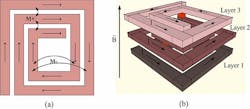
This design is a version of multi-stacked spiral solenoidal inductors. Such an inductor stacking method will enhance the inductance density of the inductor for a given area, leading to improved power density in a design.
Biomedical sensor electronics is a perfect application for powering medical sensors. This design architecture for PCB spiral inductors delivers low cost, batch fabrication, durability, and manufacturability on flexible substrates.
For example, the design and use of multi-spiral stacked solenoidal inductors for biomedical applications in the 13.56-MHz band enhances an inductor’s inductance density. Applications include wearable and implantable sensor types. The use of batteries for a power supply isn’t appropriate for medical implantables or for under-the-skin use because they can possibly contaminate the blood. An alternative for powering implantable circuits would be to supply power wirelessly for tether-less and battery-less operation of these circuits on a small PCB (Fig. 6).
An Efficient High-Power-Density PCB Embedded Inductor
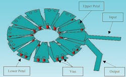
This section will examine the design and implementation of a high-power-density, and highly efficient, air-core embedded inductor onto a PCB. The design architecture is for a 280 W-5 A/240 nH; 280 W-12 A/150 nH; and 280 W-18 A/50 nH power supplies. This toroidal PCB embedded inductor has the advantage of reducing EMI effects in the converter circuit design. Figure 7 shows the geometry of a PCB embedded inductor.
The PCB embedded inductor will attain a higher power density via the miniaturizing of the associated components due to increasing the resistance. However, this will lead to losses such as copper conduction loss.
There’s a tradeoff between higher power density and higher efficiency in a PCB embedded inductor. In the optimum circuit design, the power design operates at a high 18-A current with very low resistance (dc: 2.5 mΩ/ac: 8 mΩ). This results in a high-power-density/efficient toroidal PCB embedded inductor without the use of a heatsink. That current inductor in particular achieves the benefit of integration and miniaturization of the passive filter for high-frequency wide-bandgap converters.
Summary
Designers can use numerous techniques to minimize board space while improving power density in their designs. This article mentions and explains a few of the most useful stacked-inductor architectures that help circuit designers achieve high power density. Each of these designs have tradeoffs that the designer must consider to meet circuit design goals.
Read more articles in the Power Management Series: Delving Into Power Density
References
1. “A Passive-Stacked Third-Order Buck Converter With Inherent Input Filtering Achieving 0.7-W/mm2 Power Density and 94% Peak Efficiency,” IEEE Solid-State Circuits Letters, Vol. 2, NO. 11, NOVEMBER 2019.
2. “LDC0851 Stacked Coil Design Considerations,” Application Report SNOA982–February 2018.
3. “Resonance and EMI in Vertical Multi-coupled Coils for Wireless Power Transfer (WPT) System,” IMWS-IWPT2012 (International Microwave Symposium Series - Innovative Wireless Power Transmission) Proceedings.
4. “Design and Optimization of Printed Circuit Board Inductors for Wireless Power Transfer System,” University of Tennessee, Knoxville.
5. “Design Considerations for High Power Density/Efficient PCB Embedded Inductor.”
6. “High Power Density Stacked-Coils Based power Receiver for MHz Wireless Power Transfer,” 2019 IEEE PLS Workshop on Emerging Technologies: Wireless Power Transfer (WoW).
