Simplify TWS Earbud Designs with 1-Wire Connectivity
Members can download this article in PDF format.
What you'll learn:
- What parts are used to create the 1-Wire TWS earbuds?
- The key role played by the DS2488 dual-port link.
- Setup for data communications.
- The design's battery management and power configuration.
The most attractive feature of true-wireless-stereo (TWS) earbuds is the convenience of wireless wear. Compared to conventional Bluetooth earbuds, TWS earbuds have many merits, such as small size, good sound quality, and high stability, as well as a certain degree of water resistance and intelligence, which have quickly caught the interest of consumers. Shipment volume and total market size for TWS earbuds continue to expand in tandem with research and development of this technology in the field of consumer electronics.
System Architecture
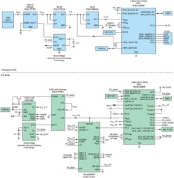
The 1-Wire TWS earbud solution presented in this article, the MAXREFDES1302, includes two parts: the charging cradle and the earbuds. The overall system hardware architecture is shown in Figure 1.
The charging cradle uses a 3.7-V, 1500-mAh, single-cell Li-ion battery to power the system, and the MAX77651 charger supporting the USB Type-C protocol to charge the battery. Users can charge the whole system via one USB Type-C cable.
For power rails, the charging cradle utilizes the MAX17224 boost module to boost the system voltage of the MAX77651 to 5 V, and the MAX38640 buck module generates 3.3 V from this 5 V to power the MAX32655 microcontroller. The 5 V also is transferred to the earbud side through the 1-Wire control circuit as the power supply that charges the earbud system.
The charging cradle uses the MAX17262 fuel gauge with an internal current-sensing resistor to monitor the battery. The MAX17262 combines the traditional coulometer with the novel ModelGauge m5 EZ algorithm; it features flexible configuration and ease of use, and no battery characterization. Furthermore, the charging cradle employs the MAX32655 with a Bluetooth 5.2 module and an internal SIMO power module as the microcontroller.
In addition to common communication interfaces, some GPIOs can be configured as a 1-Wire interface to control the DS2488 of the earbuds, providing great convenience for 1-Wire communication and charging. The SWD interface of the charging cradle can be connected to the MAX32625PICO programming platform, which updates the firmware of the MAX32655 and displays battery information on the computer through the virtual serial port. Battery information also can be displayed on the OLED screen of the charging cradle.
A 3.7-V, 130-mAh, single-cell Li-Ion battery powers the earbud. The earbud uses the DS2488 1-Wire dual-port link to implement the data communication between the earbud and the charging cradle; it also controls the 5-V charging power supply, which comes from the charging cradle.
In addition, the earbud leverages the MAX32655 microcontroller; its UART interface simulates 1-Wire timing to read and write the DS2488. The MCU similarly uses the SWD interface to connect to the MAX32625PICO programming platform to flash programs.
For power rails, the MAX77734 charger of the earbud comes with a 3.3-V LDO output to power the MAX32655. At the same time, the 3.3 V, together with the 1.8- and 1.2-V power supplies generated by the internal SIMO module of the MAX32655, forms the power rails of the MAX98050 audio codec. The earbud also uses the MAX17262 fuel gauge to monitor the battery.
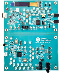
Figure 2 shows the design. The actual size of the charging cradle is 10.20 × 5.80 cm, and that of the earbud is 10.20 × 6.50 cm. Since this is a prototype to assist customers in design, testing, and research, the product size could be further diminished if the test points are simplified to meet the size requirements of actual TWS earbud applications.
1-Wire Data Communication and Power Transfer
In TWS earbud applications, it’s very important to realize reliable and convenient data communication and power transfer between the charging cradle and the earbud. Many common TWS earbuds currently on the market usually use three or more touch points to connect to the charging cradle to exchange messages and transfer power.
However, having too many touch points usually contributes to higher system cost, which is extremely detrimental to low-cost wearable products. In addition, more touch points usually require larger size, which is contrary to the small-size requirement of TWS earbuds. On top of that, more touch points tend to increase the likelihood of system failure.
Faced with these difficulties, the design presented here uses Analog Devices’ 1-Wire dual-link port, the DS2488, which is specially designed for TWS solutions to conduct power transfer and data communication between the earbud and the charging cradle. The DS2488 supports the 1-Wire protocol and can exchange data and transfer power by a single wire.
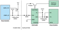
Since the system needs an additional touch point to connect the GND of the earbud and that of the charging cradle, the whole solution only needs two touch points. This can significantly improve the reliability and reduce the size and cost of the system. Figure 3 shows the block diagram of the 1-Wire communication and charging circuit of this design.
Working Principle of the DS2488
As depicted in Figure 3, the DS2488 is the 1-Wire dual-port link with two 1-Wire communication pins, IOA and IOB, which are controlled by the microcontrollers on both sides. The IOA pin is controlled by the microcontroller of the charging cradle, and the IOB pin is controlled by the microcontroller of the earbud. The IOA pin can support input voltage up to 5.5 V, as well as support different communication and charging levels on the 1-Wire bus (IOA).
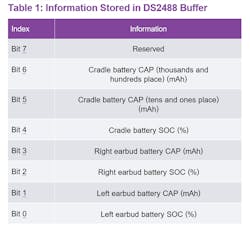
As a 1-Wire device, each DS2488 has a unique 64-bit ROM ID for users to identify and authenticate. The DS2488 also features an internal 8-byte buffer that can be read and written by the microcontroller to update battery information on both sides in real-time. Table 1 lists the information stored in the buffer.
The TOKEN pin of the DS2488 indicates the control status of the DS2488: TOKEN logic low indicates that the microcontroller on the charging-cradle side has obtained the control authority of the DS2488, while TOKEN logic high indicates that the microcontroller on the earbud side obtained the control authority of the DS2488.
The CD/PIOC pin of the DS2488 controls the charging cradle to charge the earbud. When the voltage on the 1-Wire bus (IOA) is lower than 4 V, the CD/PIOC pin is high impedance, so the transistor is off and charging stops. When the voltage on the 1-Wire (IOA) is higher than 4 V, the CD/PIOC pin is logic low. The transistor is on, so the voltage on the 1-Wire bus (IOA) is directly transferred to the charger of the earbud, and charging starts.
The MOSFET connected to 5 V determines when to charge and when to communicate. The turn-on and turn-off of the MOSFET is controlled by the microcontroller of the charging cradle. The usage of the earbuds and charging cradle can be roughly divided into the following three cases:
The earbud is in the cradle and the cradle cover is open
In this case, the microcontroller of the charging cradle turns off the MOSFET and obtains the control authority of the DS2488. Under these circumstances, the TOKEN pin is logic low and the CD/PIOC pin is high impedance. The charging cradle reads the 8-byte buffer of the DS2488 through the 1-Wire bus (IOA) to read the earbud battery information and writes the 8-byte buffer to update the cradle battery information. At this time, charging stops and communication starts.
The earbud is in the cradle and the cradle cover is closed
In this case, the microcontroller of the cradle turns on the MOSFET, so 5 V is directly transferred to the earbud through the 1-Wire bus (IOA). Under these circumstances, the TOKEN pin is logic high and the CD/PIOC pin is logic low. The 5 V from the cradle is transferred to the earbud side to charge the earbud battery.
Meanwhile, the microcontroller of the earbud obtains the control authority of the DS2488, updates the earbud battery information, and reads the cradle battery information by reading and writing the 8-byte buffer of the DS2488 through the 1-Wire bus (IOB). At this time, communication stops and charging starts.
The earbud isn’t in the cradle, or the cradle battery is nearly dead
In this case, the 1-Wire bus (IOA) is high impedance, the TOKEN pin is logic high, and the CD/PIOC pin is high impedance. Here, the microcontroller of the earbud obtains the control authority of the DS2488 and updates the earbud battery information by writing the 8-byte buffer of the DS2488 through the 1-Wire bus (IOB).
DS2488 1-Wire Data Communication
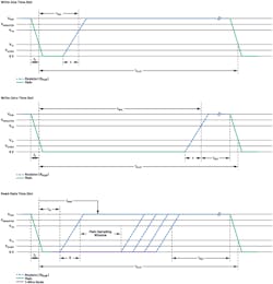
As mentioned, this design uses the DS2488 as a bridge between the microcontrollers on the charging-cradle side and the earbud side to realize the message exchange on both sides. The DS2488 supports the typical 1-Wire communication protocol. The protocol includes reset and response timing and read/write timing. The read/write timing includes a write-zero slot, a write-one slot, and a read-data time slot (Figs. 4 and 5). Timing slot duration details are listed in the DS2488 datasheet.
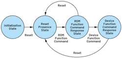
All 1-Wire devices have an internal state machine; its state transition diagram is shown in Figure 6. As seen in Figure 4, when the microcontroller sends a reset signal to the DS2488, the 1-Wire bus will be pulled low for 48 to 80 μs, and then the bus will be released to high level by the pull-up resistor. If there is a DS2488 on the bus, the DS2488 will respond to the reset signal and pull the 1-Wire bus low again for 6 μs to 10 μs after the bus is released for 48 μs.
At this time, the microcontroller can detect the level change on the bus. That is, it’s able to determine whether there’s a DS2488 connected to the 1-Wire bus by detecting whether the bus is pulled low again.
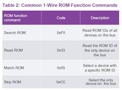
Once the DS2488 has responded to the reset signal, the microcontroller will send a ROM function command. All 1-Wire devices have the same ROM function commands. Some common ROM function commands are summarized in Table 2.
In the design, two DS2488s are connected to the 1-Wire bus (IOA) because two earbuds are typically in the charging cradle. The read ROM command (0x33) and the match ROM command (0x55) are used to read the ROM IDs of the two DS2488s on the 1-Wire bus (IOA). They also match the DS2488 with the specific ROM ID to implement the identification and selection of the left earbud or the right earbud.
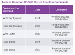
After sending the ROM function command, the microcontroller will send a device function command to perform further control of the device. Different 1-Wire devices have different device function commands. For the DS2488, some common device function commands are summarized in Table 3. This design uses the write buffer (0x33) and the read buffer (0x44) commands to read and write the 8-byte buffer of the DS2488 to realize battery information exchange between the charging cradle and the earbud.
Two groups of GPIOs (P0.6 and P0.7, P0.18 and P0.19) of the cradle’s MAX32655 microcontroller can be configured as the OWM_IO pin and the OWM_PE pin of the 1-Wire module to realize communication to the DS2488 and 5-V transfer, respectively. In this design, the OWM_IO pin of the MAX32655 is connected to the IOA pin of the DS2488 to realize 1-Wire communication function between the cradle’s microcontroller and the DS2488 of the earbud.
On another front, because some microcontrollers on the market don’t have the 1-Wire interface, for the convenience of design, the earbud’s MAX32655 MCU uses the UART interface to simulate 1-Wire timing and communicates with the DS2488 through the IOB pin (Fig. 3, again). The MCU can realize this function by configuring a specific UART baud rate and sending a specific code pattern.
Taking the reset and presence sequence shown in Figure 4 as an example, when the baud rate is 115200, the duration for the UART to send or receive 1-bit data is about 8.68 μs. Therefore, the duration for 1-byte data is approximately 69.44 μs. Since 0xE0 (11100000, LSB first) exactly corresponds to the 1-Wire reset timing, it can be sent as the 1-Wire reset signal.
Thus, if the MCU sends 0xE0 (1-Wire reset signal) through the TX pin, the DS2488 on the 1-Wire bus (IOB) will respond to this 1-Wire reset signal and pull the bus low for 6 to 10 μs. At this time, the signal received by the RX pin should be 0xC0 (11000000) or 0x80 (10000000). To conclude, the microcontroller can implement the function of simulating 1-Wire timing via UART by sending and receiving different code patterns and comparing the received and sent signals.
DS2488 1-Wire Power Transfer
As shown in Figure 3, the OWM_PE pin of the cradle’s MAX32655 MCU controls the turn-on and turn-off of the MOSFET. When the MOSFET is off, the system conducts 1-Wire communication. When the MOSFET is on, the 5 V voltage is transferred to the earbud side through the 1-Wire bus (IOA). As soon as the DS2488 detects 5 V, the CD/PIOC pin will output low level to turn on the transistor to transfer the 5 V to the MAX77734 charger to charge the earbud battery.
Battery Management and Power Configuration
The battery management and power configuration system of the charging cradle consists of the MAX77751 USB Type-C charger, the MAX17262 fuel gauge, the MAX17224 boost dc-dc converter, and the MAX38640 buck dc-dc converter.
Generally, the termination voltage of a single-cell Li-ion battery is 4.2 V, so MAX77751CEFG+ is selected as the specific part number of the charger. Its charging current is configured by the resistors connected to the IFAST pin and the ITOPOFF pin. Considering the design needs, a fast charge current of 500 mA and a top-off current of 100 mA are selected, and the corresponding resistors are 2.4 kΩ and 8.06 kΩ, respectively.
The MAX17262 fuel gauge features the ModelGauge m5 EZ algorithm, which can automatically measure the battery after configuring battery parameters such as battery capacity, termination current, and charging voltage threshold, without additional battery characterization. The output voltages of the MAX17224 and the MAX38640 are respectively configured by resistors connected to the SEL pin and the RSEL pin. In this design, 0-Ω and 56.2-kΩ resistors are selected to output 5 V and 3.3 V, respectively.
The battery management and power configuration system of the earbud consists of the MAX77734 charger and the MAX17262 fuel gauge. The output of the MAX32655 microcontroller SIMO module also provides 1.8- and 1.2-V power rails for the system.
Since only one 3.3-V LDO output is needed, the MAX77734GENP+ is selected as the specific part number of the charger. The charger also can be configured to factory-ship state, shutdown state, and standby state through I2C to extend battery life. The MAX32655 microcontroller provides four SIMO outputs, each of which can be configured to output different voltages.
Firmware Design
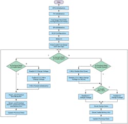
Figure 7 shows the flowchart of the charging cradle firmware. After power-on, the charging cradle’s microcontroller will initialize GPIOs and configure the MAX17262 fuel gauge and OLED module. Then, the microcontroller polls the status of the cradle cover. If the cradle is closed, the microcontroller will disable the 1-Wire module and apply the 5-V charging voltage to the 1-Wire bus (IOA) to charge the earbud. In this case, if the microcontroller detects that the remaining power of the cradle battery is less than 5%, charging will be stopped.
If the cradle is opened, the microcontroller will disable the 5-V charging voltage and enable the 1-Wire module to read and write the DS2488 buffer. Battery information of the cradle and earbud is displayed through an OLED module or the virtual serial port.
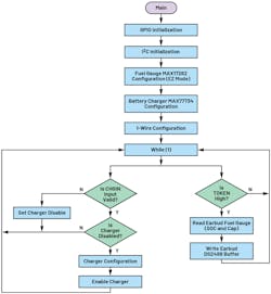
A flowchart of the earbud firmware is shown in Figure 8. After power-on, the microcontroller of the earbud will initialize GPIOs and configure the MAX17262 fuel gauge and the MAX77734 charger. Then, the microcontroller polls whether the input voltage from the charger is valid. If the input voltage is valid and greater than 4 V, the microcontroller enables the charger and starts charging.
Subsequently, the microcontroller polls the status of the TOKEN pin. If the TOKEN pin is logic low, the cradle has the control authority to read and write the DS2488. If the TOKEN pin is logic high, the earbud has the control authority to read and write the DS2488. Under these circumstances, the microcontroller writes the earbud battery information into the buffer of the DS2488 for the cradle to read.
Test Results
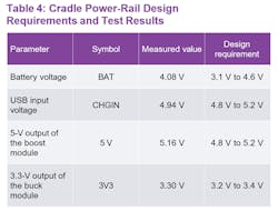
The design requirements and test results of the power rail of the cradle and earbud are shown in Tables 4 and 5. This design can meet the system design requirement.
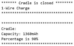
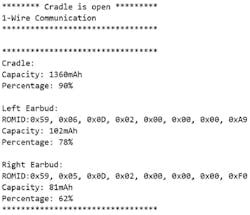
The test results for the open cradle and closed cradle are shown in Figures 9 and 10, respectively. This design can display the information of the cradle battery and earbud battery in real-time, as well as read and display the ROM ID of the DS2488 of the earbud.
Conclusion
Prototyping TWS earbud solutions is a challenge that requires the balance between ease of use, low cost, portability, and stability. The DS2488 1-Wire dual-port link paves the way for low-power, high-stability, high-performance TWS earbud solutions in smaller form factor and at a lower cost. Building on the DS2488, the MAXREFDES1302, including hardware design and firmware design, is an easy-to-use TWS earbud prototype that’s capable of power transfer and data communication through only two touch points.
References
Fang, Liang and Ning Jia. “MAXIM PLC Technology-Based TWS Solution.” Electronic Engineering & Product World, May 2021.
MAX32655 User Guide. Maxim Integrated, March 2021.
About the Author
Yi Xin
Applications Engineer, Analog Devices Inc.
Yi Xin is a member of the technical staff at Analog Devices and is responsible for support and application of healthcare biosensor products. He graduated from Fudan University and the Chinese University of Hong Kong, with a Bachelor of Science in electronic information science and technology and a Master of Science in electronic engineering, respectively. Yi joined Maxim Integrated (now part of Analog Devices) in 2018.
Voice Your Opinion!
To join the conversation, and become an exclusive member of Electronic Design, create an account today!

Leaders relevant to this article:

