Buck Regulators Quench Current-Loop Transmitter’s Power Thirst
Members can download this article in PDF format.
What you'll learn:
- Replacing linear regulators with high-voltage buck converters in current loops.
- Steps involved to make the regulator swap.
- What is burst mode?
Autonomous control is increasingly prevalent in industrial and consumer applications, but even cutting-edge autonomy solutions rely on an old technique—the current loop. Current loops are a ubiquitous component in control loops that work both directions. They convey measurements from sensors to programmable logic controllers (PLCs) and conversely convey control outputs from the PLC to process modulation devices.
The 4- to 20-mA current loop is the dominant industry standard for accurate and reliable transmission of data via a twisted-pair cable from remote sensors to a PLC. Simplicity, longevity, robustness, proven reliable data transfer over long distances, good noise immunity, and low implementation cost suit this interface for long-term industrial process control and automated monitoring of remote objects in noisy environments.
Traditionally, power for current loops is supplied through linear regulators for many of the previously listed reasons. The downsides to using linear regulators—when compared to switching regulators—are their relative inefficiency and limited current capability. Inefficiencies can lead to heat-dissipation problems and limited current often precludes the addition of desired control-system functionality.
New high-efficiency, high-input voltage buck regulators are robust and small enough to replace linear regulators in many current-loop systems. The advantages of a buck over a linear regulator are many, including higher current capability, wider input ranges, and higher system efficiency. Significant performance advantages can be found in buck regulators that feature low minimum tON times at high switching frequencies, yielding compact, robust solutions.
Background
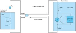
The standard 4- to 20-mA current loop shown in Figure 1 can be used to carry sensor information from field instrumentation as well as control signals to the process modulating devices, such as a valve positioner or other output actuator. It consists of four components:
- Current-loop power source: The power-supply VDC voltage varies (9 VDC, 12 VDC, 24 VDC, etc.) depending on the application, with at least 10% higher potential than the voltage drop of the combined components in the circuit (e.g., transmitter, receiver, and wires). This VDC is tapped by local step-down regulators to supply power to sensors and other components.
- Transmitter: The main component of the transmitter is the sensor or transducer. It converts a physical signal, such as temperature, pressure, current, distance, or a magnetic field, into an electrical signal. If the converted signal is an analog voltage, a voltage-to-current converter that’s part of the transmitter is required to convert it to a 4- to 20-mA current signal. In the case of a smart-digital output sensor, a DAC converts the digital signal back to an analog signal. A local power supply in the transmitter—LDO or buck regulator—powers all of the analog, digital, and reference circuits.
- Receiver or monitor: The receiver converts the 4- to 20-mA current signal into a voltage signal, which can be further processed and/or displayed. The conversion of the current signal to useful voltage levels is via a high-precision shunt resistor (RSHUNT) and/or analog-to-digital converter or data-acquisition circuit. In the instrument terminal, local buck regulators power the receiver circuits.
- 2- or 4-wire loop: A complete current-loop circuit can stretch over 2,000 feet comprises the series-connected transmitter, power supply, and receiver. In two-wire 4- to 20-mA current loops, the power supply shares the same loop with the current loop.
For example, to measure 0 to 50 psi of pressure using a remote pressure transducer, the 4- to 20-mA current receiver circuit is in series with the pressure-to-current transducer. At the sensor side, it reads 4 mA when the pressure is 0 psi, and 20 mA when the pressure is 50 psi. At the receiver side, Kirchhoff’s first law tells us that an identical current appears at the shunt resistor, where it’s converted to a voltage signal.
Autonomous operations in industry, refinery, highway monitoring, and consumer applications require high-performance sensor technologies and reliable, accurate current loops to convey sensor information. The components of the current loop must maintain high accuracy, low power, and reliable operation over an extended –40 to +105°C industrial temperature range, with required security and system features.
The source voltage at the transmitter (sensor) side can be up to 65 V during transients, which must be converted down to 5 V or 3.3 V. As the sensor circuitry is often designed to draw power directly from the current loop (no additional, local power source), it’s typically limited to 3.5 mA.
When more functionality and features are added at the transmitter, this limit becomes a problem when traditional linear regulators are used, which can’t provide any additional current. Furthermore, most of the power in the system using a linear regulator must be burned in the regulator itself, producing significant heat in an encapsulated system.
The LT8618 extends the input range to 65 V and expands the load capability to 15 mA. Its high efficiency takes the thermal constraint out of the current-loop system design where the transmitters are encapsulated and exposed to harsh environmental variations. A low-cost filter is proposed to reduce the voltage ripple and the cable side current ripple. This article analyzes the performance of the power regulator and provides the component selection guideline to meet rigorous industrial requirements. Test data for efficiency, startup, ripple, etc. are provided.
Closing the Current Loop Using a Buck Converter
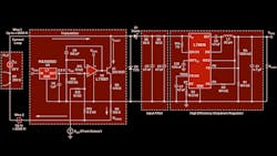
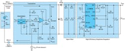
The LT8618 is a compact buck converter with a lot of features that meet the requirements of industrial, automotive, and other unpredictable power-source environments. It readily fits 4- to 20-mA current-loop applications, with ultra-low quiescent current, high efficiency, wide input range up to 65 V, and compact size. Figure 2 shows a complete transmitter circuit solution using the LT8618 to power the MAX6192C high-accuracy reference, voltage-to-current conversion, and other circuits.
The current at the shunt circuit 2SC1623 is proportional to the voltage applied at the positive input of the error amplifier (EA). The 2.5-V reference voltage is produced by the MAX6192C, a precision reference IC with low noise, low dropout, and low temperature drift of 5 ppm/°C (max). In the case of a smart sensor with a digital output proportional to the environmental variables, a DAC can convert the digital signal to an analog signal and feed it to the error amplifier.
Therefore, with the EA, BJT (2SC1623), and 100-Ω (±0.1%) sense resistor (RSENSE), the transducer modulates the current in the current loop from 4 to 20 mA, where 4 mA represents a live zero and 20 mA represents the maximum signal. The live or elevated zero of 4 mA allows for the device to be powered even with no process signal output from the field transmitter. Hence, the current in the shunt circuit is proportional to the environmental variables, such as pressure, temperature, level, flow, humility, radiation, pH, or other process variables.
The two long wires, which are part of the information-carrying current loop, are also used to provide power to the transmitter from VDC, the power supply on the receiver side. The minimum voltage of the VDC should be enough to cover the voltage drop across the wires, shunt, and minimum operating voltage of the transmitter. The source voltage is application-dependent, typically 12 or 24 V, but can be as high as 36 V.
At the remote transmitter terminal, a Schottky diode (D1) protects the transmitter from reverse-current flow. Further protection is provided by a Zener or TVS (D2) diode placed across the input to limit transient voltage surges, which are proportional to the inductance of the current loop. The loop voltage is stepped down by the LT8618 high-efficiency monolithic buck regulator to 5.5 or 3.3 V—to power the reference, DAC, and other function blocks.
In Figure 2, the wires between VDC and the transmitter can range from several feet to 2,000 feet. The stray inductance of the current loop forms an LC resonant tank with the input capacitor of the buck regulator. A transient on the power-supply side (VDC) also appears at the remote transmitter’s input side.
For a worst-case undamped oscillation, the peak voltage can double that of the VDC. For instance, if the operating input voltage is 24 V typical with a maximum specification of 36 V, the maximum voltage on the transmitter side is at risk of going beyond 65 V. Easy protection can be implemented using a TVS diode (D2) in front of the transmitter to limit any surge during transient, as shown in Figure 2.
Alternatively, an efficient system could be built by protecting the LT8618 from high-voltage excursions with an LDO regulator. In such a topology, the LDO regulator would regulate to the input minus its dropout voltage with the LT8618 converting this ~24 V to 5 V or 3.3 V with high efficiency.
The current limit of the LDO regulator should be set below the typical 3.8 mA while also maintaining high efficiency. The input capacitor of the LT8618 basically serves both as a decoupling and reservoir capacitor as well. This would enable short bursts of high loads downstream with minimal to no current draw in the current loop.
High-voltage excursions are short, typically carrying little overall energy. The resulting power loss in the LDO regulator during these transients doesn’t impair overall efficiency. That is, the LDO regulator spends nearly all of its time at a high step-down ratio.
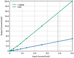
A typical current loop puts a limit on the input current of the power circuit that’s powering the complete remote transmitter. Available load current from an LDO regulator can’t exceed this input current limit. On the other hand, a buck regulator can multiply the input current supplied to the load.
Figure 3 shows output current vs. input current of the LT8618 regulator for a 24-V input to 5.5-V conversion. For an input current limit of 3.8 mA, the output current is almost 15 mA. This extra power simplifies the system designer’s job by increasing operational headroom and enabling additional functional blocks.
Burst-Mode Operation Improves Efficiency at Tiny Loads
An LDO regulator’s efficiency is proportional to the step-down ratio (VOUT/VIN) and can be efficient when the input voltage is slightly higher than the output. The problem arises at high step-down ratios, where efficiency is very low, producing significant thermal stress on the system.
For instance, with the input at 55 V and output at 3.3 V, the power loss of the LDO regulator is 0.19 W with 3.8 mA of load current. In contrast, a properly designed buck regulator can be very efficient at high step-down ratios.
Furthermore, synchronous buck regulators can increase efficiency over nonsynchronous counterparts by replacing the catch diode with a MOSFET. The challenge with a synchronous buck converter is optimizing the efficiency over the entire load range—specifically, at light loads of 3 to 15 mA, when the input can be as high as 65 V.
For a typical synchronous buck converter, three power losses dominate: switching losses, gate-drive loss, and losses associated with the converter IC controller logic circuit. Switching and gate-drive losses can be significantly lowered if the switching frequency is reduced, so simply running the converter at low frequency diminishes the switching and gate losses at light loads.
At light loads, the bias loss of the logic circuits is on par with the relatively low switching-related losses. The bias circuit is normally powered from the output, only taking power from the input via an internal LDO regulator during startup and other transient conditions.
The LT8618 addresses logic circuit losses at light loads by operating in “burst mode.” In this mode, current is delivered in short pulses to the output capacitor, followed by relatively long sleep periods, where most of the logic control circuits are shut down.
To further improve the efficiency at light loads, a larger value inductor is preferred. That’s because more energy can be delivered to the output during the short switching pulses and the buck regulator can remain in sleep mode longer between those pulses. By maximizing the time between pulses, and minimizing the switching losses of each short pulse, the LT8618 quiescent current can be less than 2.5 μA while maintaining the output in regulation from inputs up to 60 V. Since many transmitter circuits draw low current most of the time, this low quiescent current is a significant energy saver over typical bucks, which draw tens or hundreds of microamps.
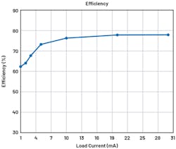
Figure 4 shows the efficiency for the current-loop solution shown in Figure 2, with the 5.5-VOUT output rail tied to the BIAS pin of the LT8618. The peak efficiency reaches 87% at the full 100-mA load, with 28-V input and an 82-µH inductor. The 10-mA load efficiency at or above 77% for the same 28-V input is arguably more impressive.
Input Filter to Limit Both Inrush Current and Current-Loop Ripple
The input of the power regulator is connected to the current loop, so it’s important to limit the ripple current and inrush current during startup or load transients as well, in addition to the steady-state current limit. The inrush current during startup of a power converter depends on the sizes of the input and output capacitors for a given soft-start time. This is the tradeoff: Minimize the input capacitor to prevent large inrush currents while making it big enough to maintain acceptable low ripple.
The input current of a buck converter is pulsed; therefore, the input capacitor plays a key role in providing a filter path for the ripple current. Without this capacitor, a significant amount of ripple current would flow through the long current loop, causing the buck to behave unpredictably. Thus, there’s a minimum input capacitance that meets ripple-current and ripple-voltage requirements. Multilayer ceramic capacitors (MLCCs) have the best performance with regards to ripple current due to their low equivalent series resistance (ESR) and equivalent series inductance (ESL).
When the converter operates in burst mode, the inductor current follows a triangular waveform. The impedance of the current loop is much higher than the input filter. Therefore, the ripple voltage across the input capacitor can be estimated by the following equation, ignoring the capacitor’s ESR and ESL, where IPEAK is the burst current in the buck inductor, and VR is the ripple voltage across the input capacitor (obviously a bigger capacitance is needed for higher burst currents):
To minimize the input voltage ripple while keeping the input capacitance as small as possible, we prefer a smaller buck inductance. Nevertheless, burst-mode efficiency is better with a large inductor. For an 82-µH inductance and 1-V ripple, to avoid triggering UVLO at any minimum input instance, a 100-nF input capacitor is sufficient for this application using the LT8618.
Most of the ripple current goes through the local decoupling capacitor, and the residual portion shares the same path as the current loop. It’s important to keep the current ripple in the cable side small since it will appear across the shunt sense resistor as voltage ripple—the magnitude of the voltage ripple must be smaller than the resolution spec of the ADC reading the voltage across the shunt sense resistor.
The current ripple can be further reduced by employing additional filters. An RC filter is a good design tradeoff because the input current is small, and it’s low cost compared to an LC filter. Smaller ripple currents also can be achieved with two or three cascaded stages of RC filters.
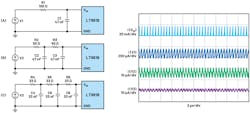
LTspice simulations allow us to compare the current ripple at the source cable side for three different input filter structures, with a total resistance of 100 Ω in series in the input path (Fig. 5). It can be accomplished by using the LT8618 with VIN = 28 V and VOUT = 5.5 V, and an 82-µH inductor. A current pulse is equivalent to what the input filter would see as input current to the LT8618 regulator for 10 mA of output current.
A single-stage RC filter with 100 Ω and 100 nF has a current ripple of more than 60 µA peak-to-peak at the source cable side. The ripple current at the source cable side becomes smaller as more capacitance is added or filtering stages are cascaded. Given that a buck regulator performs better with a bigger direct input capacitor, and that a two-stage RC filter has a smaller BOM than a three-stage option while delivering similar current ripple at the source cable side, we recommend the two-stage filter with 50 Ω and 47 nF per stage.
The source-cable-side ripple current is about 30 μA, and correspondingly it produces about 7.5 mV of ripple voltage across the 250-Ω shunt resistor, which is almost enough for an 8-bit resolution ADC. To further reduce the cable-side ripple current, bigger capacitance can be used in the filters. For instance, if the 47-nF caps are replaced by 100-nF caps, the cable-side ripple current can be reduced to just 7 µA, corresponding to a ripple voltage of 1.75 mV.
In typical current-loop applications, customers would specify a current limit during startup (3.2 mA, for instance), with the exception of a specified short period of time where this limit could be exceeded. In a buck converter, a high inrush current is common to charge up the input capacitors.
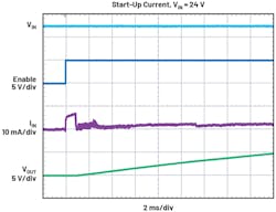
The function of the input filter is two-fold: In addition to limiting the ripple current at the cable’s source side, it also helps limit the startup inrush current. Figure 6 shows the input current over time during the startup behavior with the two-stage input filter, for an input VIN of 24 V and 4 mA of load current at the output side.
Conclusion
Current loops are widely used in industrial and automotive systems to collect and transmit information from sensors to control systems, sometimes over relatively long wires. Conversely, the loop transmits controller outputs and modulation instructions to remote actuators and other devices. Significant efficiency and performance improvements can be realized by improving the power supplies in the current loop, notably by replacing traditionally used linear regulators with high-efficiency buck regulators. This also increases current capability and expands input ranges.
High-efficiency, high-input voltage regulators in tiny packages with low minimum on times make it possible to produce compact overall solutions, comparable in size and robustness to LDO regulator solutions. This article showed how to use the LT8618 in a 4- to 20-mA current-loop transmitter, meeting rigorous industrial requirements.
References
Brant, James. “Ask the Applications Engineer—10: About Wire.” Analog Dialogue, Vol. 25, April 1991.
Loquinario, Jino and Paul Blanchard. “AN-1344: High Common-Mode Voltage Current Loop Transmitter Front End.” Analog Devices Inc., October 2015.
