The Top Switching Converter Topologies for High Power Density

This article is part of the Power Management Series: Delving Into Power Density.
Members can download this article in PDF format.
What you'll learn:
- The three-level, three-phase SiC AC-DC architecture.
- T-type inverter and T-Type inverter with SiC MOSFETs topologies.
- Totem-pole topology implemented with SiC or GaN.
High power density has steadily ramped up since the latter part of the 1980s. Power converters are ever being made smaller in size and lower in weight. Good reasons for this miniaturization trend stem from demands in applications such as aerospace and satellites, and biomedical devices. And the industry continues to try to meet customer needs for portable power-supply devices like uninterruptible power supplies (UPS), desktop and laptop power supplies, portable battery chargers, power for telecom, information technology, and data servers.
What are some of the high-power-density power-supply design architectures that stand out in the industry? Let’s take a look.
10-kW/10-kVA Three-Level, Three-Phase SiC AC-DC Reference Design
This switching power converter design from Texas Instruments (TI) will enable power designers to implement a three-phase, 10-kW/10-kVA, three-level, AC-DC, bidirectional functionality power converter, having digital control (Fig. 1).
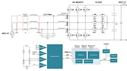
The switching frequency of 50 kHz, using silicon-carbide (SiC) MOSFETs, will shrink the magnetics for the filter design, leading to a higher-power-density converter design. SiC MOSFETs with lower switching losses, and a low peak efficiency of more than 97%, will be minimized to enable DC bus voltages as high as 800 V.
T-Type Inverter
Each leg of a T-type inverter has four active switches and this module commercially available even with using wide-bandgap (WBG) semiconductor devices like SiC or gallium-nitride (GaN) devices (Fig. 2). While the commercial availability of T-type inverter leg modules are more compact and lower cost, the use of WBG semiconductors will greatly increase their efficiency.
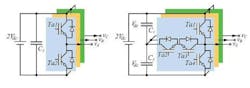
10-kW T-Type Inverter Using SiC MOSFETs
A T-type inverter is quite close in design to the three-level neutral-point clamped (NPC) inverter.5 The key features of the NPC inverter are reduced dv/dt and lower total harmonic distortion (THD) in the AC output voltages.
Compared to the two-level inverter, the NPC inverter has an additional output voltage level at 0 V, thus enabling improved harmonic performance over a standard two-level inverter. The T-type inverter also has a lower parts count due to the elimination of clamping diodes, along with reduced conduction losses of the outer switching devices (this is because only one device is used instead of two in series).
The T-type inverter has a disadvantage in that the blocking voltage is lower than the NPC inverter because the outer switching devices are now no longer in series. This can be overcome by employing modern WBG devices.
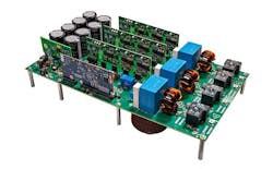
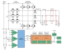
Figure 3 depicts TI’s TIDA-01606 10-kW, bidirectional, three-phase, three-level (T-type) inverter and power-factor-correction (PFC) reference board design. Figure 4 shows the schematic of the inverter.
GaN vs. SiC Power-Density Performance
Renewable power and electric vehicles demand high power density as well as high efficiency.
In this vein, the dual-boost topology (Fig. 5a) is a popular choice in high-power systems that exceed 1 kW. The introduction of SiC diodes, along with the latest generation of superjunction (SJ) MOSFET transistors, brought much sought after improvements in power density and efficiency. However, these gains have reached a plateau in the last 13 years.
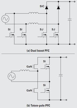
A totem-pole topology (Fig. 5b) can be a cost-effective alternative to the dual-boost PFC topology. It reduces the number of power devices and inductors by 50%, while significantly increasing the density and efficiency of the design.
Totem-pole solutions can include power elements that use either SiC or GaN devices. GaN offers some advantages over SiC in this topology:
- Zero reverse recovery: Unlike MOSFETs, GaN FETs have no P-channel or N-channel junction within their lateral structure. This means that there are no body diodes or associated reverse-recovery losses in MOSFET devices. SiC FETs experience reverse-recovery losses in their body diode. A typical SiC FET has greater than 85 nC of reverse-recovery charge.
- Lower switching energy: Switching energy of GaN devices is more than 50% less than that of SiC devices, leading to lower losses in the PFC stage. GaN is able to achieve switching frequencies higher than 1 MHz in critical totem-pole applications.
- Faster switching speeds: The latest generation of GaN devices, which have integrated gate drivers, are able to switch as fast as 150 V/ns. This results in an 82% reduction in losses when compared to SiC devices, and a reduction in losses of 63% versus discrete GaN FETs.
- Lower dead-time losses: While in PFC-mode operation, there will be a short period in each switching cycle known as “dead time.” This means that neither of the two switches in the half bridge will be turned on. The duration of this dead-time period, and the associated voltage and current, will directly result in losses during each cycle. These losses can be lowered via a complex control algorithm, such as adaptive dead time. With the availability of advanced driver features, like the ideal-diode mode, it’s possible to lower dead-time losses by more than 67%, as compared to both SiC and discrete GaN implementations, with no need for complex firmware or hardware control.
Figure 6 shows a loss breakdown between a dual-boost SJ PFC, a totem pole with SiC power devices, and a totem pole with GaN power devices. In this application, GaN will have the lowest losses with the highest efficiency. These advantages enable designers to achieve high-power-density designs, while significantly reducing the size and cost of the necessary cooling components like fans and heatsinks.

Summary
When MOSFET power transistor devices appeared on the scene, power circuit designers were able to enhance their power electronics designs as never before. Fast forward to the introduction of GaN and SiC power devices, designers now had new tools with which power designs could reach new levels of performance. Higher voltage and current capabilities emerged along with higher efficiency and higher figure of merit (FOM) switching.
A price disparity still exists between SiC and GaN switches. Thus, designers will make their choices depending on their application and other system considerations, such as energy savings over time from savings in efficiency.
Read more articles in the Power Management Series: Delving Into Power Density.
References
1. “A review on enabling technologies for high power density power electronic applications,” Science Direct, materialstoday: Proceedings, Volume 46, Part 9, 2021, pg. 3888-3892.
2. “10kW/10kVA Three-Level, Three-Phase SiC AC-DC Reference Design,” Texas Instruments, 2019.
3. “A 100kW Forced-Air-Cooled SiC MOSFET Converter Achieving a Power Density of 1.657kW/L and an Efficiency over 98.5%,” 2020 IEEE 9th International Power Electronics and Motion Control Conference, IPEMC2020-ECCE Asia.
4. “Three-phase, three-level, T-type, grid-connected inverter with reduced number of switches,” 6th International Istanbul Smart Grids and Cities Congress and Fair (ICSG), 2018.
5. “Multilevel Inverters, Introduction and Emergent Topologies, Chapter 2 - Neutral-point-clamped and T-type multilevel inverters,” Academic Press, 2021.
About the Author

Steve Taranovich
Freelance Technical Writer, Phoenix Information Communication LLC
Steve is a contributing editor to Electronic Design.
Author of the non-fiction “Guardians of the Right Stuff,” a true story of the Apollo program as told by NASA and Grumman Corp. engineers, an astronaut, and technicians.
Experienced Editor-In-Chief of EETimes/Planet Analog and Senior Technical Editor at EDN running the Analog and Power Management Design Centers from 2012 to 2019.
A demonstrated history in electronic circuit design and applications for 40 years, and nine years of technical writing and editing in industry. Skilled in Analog Electronics, Space-related Electronics, Audio, RF & Communications, Power Management, Electrical Engineering, and Integrated Circuits (IC).
1972 to 1988 worked as a circuit design engineer in audio (8 years) and microwave (8 years). Then was Corporate Account Manager/applications engineer for Burr-Brown from 1988 to 2000 when TI purchased Burr-Brown. Worked for TI from 2000 to 2011.
Strong media and communication professional with a BEEE from NYU Engineering in 1972 and an MSEE from Polytechnic University in 1989. Senior Lifetime member of IEEE. Former IEEE Long Island, NY Director of Educational Activities. Eta Kappa Nu EE honor society member since 1970.
Comment About the Article
To join the conversation, and become an exclusive member of Electronic Design, create an account today!

Leaders relevant to this article: