MCUs Bring Smart Cost/Performance Solutions to Intelligent Systems
Download this article in PDF format.
As sensor networks and applications become increasingly intelligent, the need intensifies to process greater amounts of data. More and more products are being connected to a central network for data collection, system monitoring, and control. This could range from an industrial temperature sensor used to monitor a factory process, an intelligent fire-detection system, or a Wi-Fi home thermostat.
Each of the above applications benefit from having a central node, which is responsible for much of the deterministic computing and large amount of number crunching while still wirelessly talking to the smaller nodes. The smaller nodes are responsible for gathering the large amounts of data.
However, this system concept can be costly in terms of power and implementation. More nodes in the system typically translates into an exponential increase in total system power. Wirelessly transmitting data can quickly consume power, and the less time spent sending data wirelessly means more time spent in lower power modes. With the burgeoning Internet of Things (IoT), there’s greater pressure on the power constraints of applications. How can this pressure be addressed?
Getting to the Core
More often than not, engineers address power concerns by looking to the core of the system, whether it’s a microcontroller (MCU), a low-end digital signal processor (DSP), or a field-programmable gate array (FPGA). The system needs to be low power enough to give a sustainable lifetime for a battery in an application, but still enable wireless communication, data measurements, and sometimes data analytics without breaking the bank on cost and complexity. Very frequently, product engineers are quick to opt for a low-end DSP engine or an FPGA and avoid MCUs, as running traditional signal processing algorithms implemented in C-code can be extremely time-intensive and power-hungry.
However, there are some significant downfalls to using a low-end DSP or an FPGA. Lower-performance DSPs can cause the overall system cost to be quite high compared to that of an MCU. When designing an application with a DSP, often times there is a need for some sort of external memory to store data. There might also be a need for a standalone analog-to-digital converter (ADC), as many DSPs do not have built in ADCs. This can add cost in a variety of ways:
- Overall bill-of-materials (BOM) cost
- Board space and layout costs
- Application design team cost.
Overall, the BOM can end up being pretty expensive when incorporating a DSP with an ADC and external memory, plus whatever extra passive components are needed. Since so many different components aren’t integrated, board space can suffer and quickly balloon to a large area. Finally, due to the complexity of the application, the hardware team is going to need to take extra time and care to ensure that the standalone ADC is laid out in such a way that the ADC’s performance will not be compromised. This extra time can lead to overhead cost for a development team, both on the hardware and software sides.
FPGAs can also provide a solution, but this will almost always consume more power than what’s desirable for a battery-powered system, as well as add complexity on the hardware and software development side. Therefore, this solution is used infrequently. Higher-end MCUs can be a good option, but with a higher-end MCU, the price paid for the performance margin is minimal and not very convincing.
Mulling the Move to MCUs
Many teams take the added complexity of the lower-performance DSP as a necessary evil and move on with development. However, what if there was something that could combine the performance of a DSP, with the integration that an MCU can provide and the data-logging benefits of having standalone memory? System costs would quickly go down and system performance could accelerate while still maintaining a tight power budget.
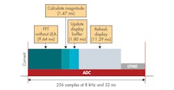
1. This FFT-based application doesn’t include a low-energy accelerator.
MCUs in the present day have integrated ADCs that can operate in lower power modes and use a direct-memory-access (DMA) peripheral to transfer that data from the ADC to somewhere in the random-access-memory (RAM) space of the MCU. This type of ADC is often easier to lay out, as integrated ADCs already take care of the finer aspects of isolating the ADC from system noise, and can generate a reference voltage (VREF), which could consume a lot of power.
Since flash is limited by its write endurance, it’s not ideal for data logging. From RAM, an MCU will send this data over a wireless network. However, this data can often be a constant stream, consuming large amounts of power to transmit, on top of the fact that RAM space is usually limited for MCUs.
If this data could be processed and the deterministic computing be done on the external node of the system instead of the central node, then less time would be spent transmitting wirelessly, thus saving more power. To help counteract the RAM size and the downside of flash, one could use an MCU that uses the ferroelectric RAM (FRAM), a non-volatile memory. FRAM has a 1015 write/erase endurance, which is magnitudes greater than the flash write/erase endurance at 104 cycles.
Hardware Accelerators
How would an MCU be able to perform against a lower-performance DSP, though? Today, MCUs are starting to see a diversifying amount of integrated peripherals that tackle new problems and provide new, never-before-seen advantages. Hardware accelerators have often been used to accelerate the performance of encryption/decryption, multiplication, and other operations for MCUs. They provide MCUs with the capability to provide a two-for-one benefit by saving power and decreasing processing time.
The latest hardware accelerators being introduced, such as the Low-Energy Accelerator (LEA) in the MSP430FR5994 FRAM MCU family, tackle signal processing. Pairing the signal-processing benefit of hardware accelerators like the LEA module with the data-logging capability enabled by the write endurance of FRAM gives birth to a new branch of solutions. In turn, it opens up a new realm of possibilities for systems in the IoT and sensors world.
In many applications, the signal-processing branch can take a large amount of time and resources to compute. Let’s look at an example. An application utilizing an MSP430 FRAM MCU without the LEA module is continually taking ADC samples using a ping-pong buffer at 8 kHz. The total time period of the application takes 32 ms. A large part of that 32 ms is spent doing a fast Fourier transform (FFT) and a magnitude calculation that’s used to do a spectral graph, which is later displayed on an LCD screen. The ADC uses the DMA to transfer to an area in the FRAM non-volatile memory space, and from there the CPU performs the calculation taking a total of 11.11 ms to compute (Fig. 1).
It’s obvious here how the signal-processing functions typically take longer on an MCU. But if we can accelerate this process through the use of hardware accelerators, then we can shorten the time it takes to do the number crunching and spend more time in lower power modes. This also helps us significantly lower the power consumption of the entire system.
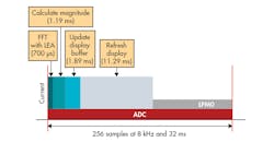
2. In this example, the FFT-based application employs a low-energy accelerator.
This exact story is proposed in Figure 2. Here, an MSP430 FRAM MCU with the LEA hardware accelerator for signal processing is used to compute the FFT and magnitude calculation. There’s a significant drop in the amount of time it takes to compute: A result is returned for the display to update in 1.89 ms, giving the application more time to spend in a low-power mode and conserve battery power. Furthermore, because it’s a hardware accelerator, the system design allows for more energy to be conserved while also performing the calculation.
Now that the performance benefits are clear, it’s important to note that the integration brings many other great benefits as well. Layout, as mentioned earlier, gets simpler as the number of passive components decreases and there are numerically less chips needed to achieve the same goal. This leads to smaller layout and less time spent both on hardware and software. Overall, this solution gives new possibilities in saving cost through simplicity, while increasing performance and lifetime.
About the Author
Voice Your Opinion!
To join the conversation, and become an exclusive member of Electronic Design, create an account today!

Leaders relevant to this article:


