ID 343923804 © Oleksandra Tsvid | Dreamstime.com
6769954db1774c330b3f0469 Chipmanufacturing Dreamstime L 343923804

Die-Attach Process Dramatically Improves Waste-Heat Removal in Power Electronics

Dec. 23, 2024
A new die-attach process promises to cool power devices up to 15X more efficiently while reducing failure-inducing stresses caused by conventional sintering techniques.

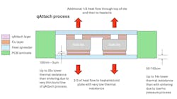
QPT just filed a patent for the “qAttach” process, a novel way to attach dies to heat spreaders or substrates (typically aluminum nitride (AlN)) that significantly reduces thermal resistance. The new assembly process also boosts reliability as it places less stress on the substrates.

Developed by QPT for use with the gallium-nitride (GaN) transistors used in its electric motor-control designs, qAttach enables the devices to more efficiently dissipate the large amounts of waste heat they generate when using them for high-power, high-voltage applications and at high frequency.

Heat removal is especially challenging for high-voltage GaN transistors because their die size is relatively small, which means there’s less surface area to remove heat from. The conventional die-attach technology is based on a sinter layer, typically 30 to 60 µm thick, which presents a relatively poor thermal path between the bottom of the die and the heatsink.

In a different approach, qAttach, which is based on a bonding material, can be applied to the top and bottom of the chip in films as thin as a single micron. The film’s low thermal resistance enables heat to be efficiently removed by a heatsink on the top of the die and by a heavy copper layer on the PCB below it. This increases thermal conduction by up to 15X, versus devices attached using conventional single-sided bonding methods. As a result, it becomes easier to use GaN devices in next-generation, high power, high-voltage applications in automotive and industrial motors.

qAttach also improves the reliability of inverter bridge modules and other assemblies containing power transistors. It does so by reducing the amount of mechanical stress the die is subjected to during the attachment process.

Reliability is further enhanced because the ultra-thin qAttach layer isn’t a laminar sheet. It has a proprietary geometry that constrains expansion predominantly in the Z axis, which is perpendicular to the qAttach layer, when heated. This virtually eliminates potential delamination of the attach layer from the die and substrate—the largest cause of failures in conventional power packages.    

Next in This Issue of PowerBites

Bourns
bourns_promo
Power

Compact Thick-Film Resistors Offer High Power Dissipation and Reliability

Bringing power ratings of up to 35 W, these rugged thick-film resistors usher in reliability and economy to industrial motor drives, AC-DC and DC-DC power converters, and battery...
Dreamstime_rzyotova_346977792 and Pulsiv
dreamstime_rzyotova_346977792
Power

USB-C Charger Design First to Deliver 240 W from Single 1C Port

A flyback-based switching architecture enables USB-C chargers to generate up to 240 W from a single 1C port.

More PowerBites

Lee Goldberg © Endeavor Business Media
powerbites_promo
PowerBites

This Week in PowerBites

Check out the latest from power technology expert Lee Goldberg.
BRM Aero | Rohm
PowerBites
PowerBites

EV V2G Standards, IGBTs Remain Relevant, First Electric Aircraft Hit the Market

While GaN and SiC enjoy the glory, advances in silicon device technology continue to make the IGBT a dominant force in power applications. Meanwhile, V2G standards get some assistance...
About the Author

Lee Goldberg | Contributing Editor

Lee Goldberg is a self-identified “Recovering Engineer,” Maker/Hacker, Green-Tech Maven, Aviator, Gadfly, and Geek Dad. He spent the first 18 years of his career helping design microprocessors, embedded systems, renewable energy applications, and the occasional interplanetary spacecraft. After trading his ‘scope and soldering iron for a keyboard and a second career as a tech journalist, he’s spent the next two decades at several print and online engineering publications.

Lee’s current focus is power electronics, especially the technologies involved with energy efficiency, energy management, and renewable energy. This dovetails with his coverage of sustainable technologies and various environmental and social issues within the engineering community that he began in 1996. Lee also covers 3D printers, open-source hardware, and other Maker/Hacker technologies.

Lee holds a BSEE in Electrical Engineering from Thomas Edison College, and participated in a colloquium on technology, society, and the environment at Goddard College’s Institute for Social Ecology. His book, “Green Electronics/Green Bottom Line - A Commonsense Guide To Environmentally Responsible Engineering and Management,” was published by Newnes Press.

Lee, his wife Catherine, and his daughter Anwyn currently reside in the outskirts of Princeton N.J., where they masquerade as a typical suburban family.

Lee also writes the regular PowerBites series

Sponsored Recommendations

Comments

To join the conversation, and become an exclusive member of Electronic Design, create an account today!