Most consumers are generally unaware that they themselves are the single biggest risk to the electronic devices they have come to depend on every day. Simply touching any device that contains sensitive electronic semiconductors can cause an electrostatic discharge (ESD) event.
A Jolting Experience
If the air around you is particularly dry, because it’s really hot or freezing cold, sliding from behind the steering wheel of your car can give you a shocking jolt when you touch the metal of the car door. The experience may be a nuisance to you, but can you imagine what that shock could do to sensitive electronic equipment?
Well, have you ever picked up your smartphone or tablet only to find that some of the buttons or data ports no longer work properly? This even bigger nuisance could be the direct result of that “jolt” penetrating your device and sidestepping its protective circuitry, instead of bouncing off the metal of your car and making you jump.
Related Articles
- Understanding ESD And EOS Failures In Semiconductor Devices
- Protect Your Fortress From ESD
- The Use And Misuse Of Circuit Protection Devices
ESD events may not be severe enough to blow up your cell phone. But if its keypad or buttons suddenly don’t work, it probably already has been damaged by an unprotected ESD occurrence. It’s just as likely that an interface port such as USB or Ethernet no longer works properly when it is connected to other devices—ESD is probably the culprit here, too.
These ESD events can be traced to a phenomenon known as triboelectric charging, which occurs when two materials make contact and are then quickly separated. Electrons are transferred between the two materials, leaving one with a positive and the other with a negative charge.
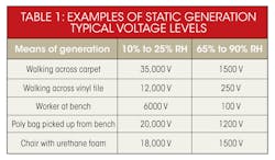
Just how high this charge is before an ESD event occurs depends on several factors, such as the area of the surfaces that make contact, how fast they separate, relative humidity, and the chemistry of the materials. ESD events take place thousands of times per day, but most of them go unnoticed unless the discharge is sufficiently severe to cause mild and brief irritation, such as walking across a carpet and grabbing a doorknob. The charges generated can range from hundreds to tens of thousands of volts (Table 1).
ESD exposure is a real problem in today’s sophisticated consumer equipment, due to ever shrinking board-level chipset size and, thus, the resulting silicon geometry via wafer processing. In this cost-sensitive manufacturing sector, ESD structures have become too large and costly to be included in the silicon IC package.
This has led IC suppliers to remove or greatly reduce the internal ESD protection offered by their product. But once these ICs are installed in consumer products, they may be subjected to ESD events that are far more severe than those reproduced for testing in controlled manufacturing environments.
Conflicting Values
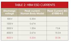
The ESD test model commonly employed by IC manufacturers, MIL-STD-883, Method 3015: Human Body Model (HBM), relates specifically to a manufacturing environment. OEMs concerned with ESD events in the field use a more stringent model defined by the International Electrotechnical Commission (IEC), IEC 61000-4-2. While most IC suppliers currently test their products at 500 V according to the HBM, OEMs will test at 8000 V (and beyond) using the IEC standard (Table 2).
The level of current in the worst case HBM ESD is much lower than that for the IEC61000-4-2 (highlighted in red on Table 2). The 8-kV event described in IEC 61000-4-2 compared to the same 8-kV event described in the HBM results in a 5.6x increase in current.
A chipset that survives HBM testing (manufacturing environment test conditions) is not guaranteed to survive in the field, where the ESD exposure will be much more severe. And considering that most IC suppliers only test to 500 V using HBM, the chipset will see a near 100-fold increase in current compared to an 8-kV ESD transient in the field, certainly sealing its fate unless ESD protection is added to the design.
Close The Gap
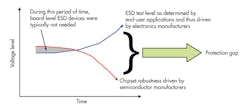
Over the last several years, application testing requirements have become more and more stringent. An ESD event of 8 kV typically now is the lowest level used. Testing levels are trending towards 20 kV and even 30 kV, while IC suppliers have continued to remove protection to save silicon area for more functionality. There is a growing need for supplementary ESD protection, represented by the “gap” between chipset ESD capability versus the ESD exposure level in the field (Fig. 1).
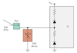
Selecting the correct ESD protection device, generally called a transient voltage suppressor (TVS) diode array, is vital for ensuring the end application will survive and continue to function as originally designed. The dynamic resistance is a very important ESD protector parameter to consider, if not the most important, when selecting a protection component.
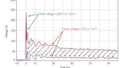
Any protection solution has an intrinsic resistance value associated with its clamping characteristic. An ideal solution minimizes the intrinsic resistance so a protection solution has the lowest impedance path to ground during a surge event (Fig. 2). During an ESD event, the clamping device will turn on or go from its nominal state of high impedance to one of low impedance.
If its series resistance is high, a high voltage (V = I*R) develops across the component, providing less effective protection for the IC. If series resistance is low, the voltage developed across the protection component is reduced and the exposure level to the IC decreases. This lower dynamic resistance (resistance value of the protection component during clamping mode) allows more of the surge current to be routed away from the IC and into ground.
Silicon Beats The Rest
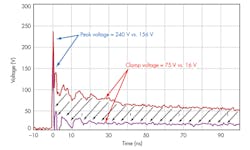
Silicon protection devices normally provide the best ESD protection due to their inherently lower dynamic resistance compared to competing technologies such as polymers and ceramics. The typical dynamic resistance of silicon components will range from 0.2 to 3.0 Ω, depending on the supplier, while ceramic-type solutions (of equal capacitance) offer dynamic resistances in the range of 2 to 5 Ω on average.
Figure 3 shows the “let-through” energy difference between a silicon ESD component and its varistor counterpart when an 8-kV ESD transient is injected into each. The leading edge turn-on difference and the final clamping voltage differences can be seen. The difference between the curves (the arrows) is the additional energy the IC or chipset must successfully survive.
International Standards
The ports, or interconnects, on consumer devices require ESD protection since they are the interface to the outside world. Some of these interfaces will require compliance to country safety standards and will need to be equipped with overcurrent and overvoltage protection. Other functions may need protection from environmental factors such as ESD, but also from nearby lightning surges or electrically fast transients (EFTs) caused by nearby high-inductive-load equipment, such as vacuum cleaners, cycling on and off.
Products that are directly connected to the ac mains (120 to 250 V ac rms) may be exposed to severe surge transients such as lightning and load switching, as well as short circuit and overload conditions. This requires a combination of overcurrent (fuses or positive temperature coefficient devices, or PTCs) and overvoltage (metal oxide varistors or MOVs, TVSs, or TVS diode arrays) components due to the severe exposure. Portable consumer products that include an ac or dc adapter may be exposed to specific ESD and low-level lightning events that must be addressed.
Keypads or other manual interface buttons may be an entry point for the destructive energy of ESD. Audio lines may have similar ESD exposure due to the speaker wire connections and manual handling. The connectors for S-video, composite video, and HDMI are also susceptible to ESD exposure due to the manual handling of such equipment parts.
Furthermore, battery pack applications will endure similar ESD exposure as well as potential “overcurrent runaway” conditions that must be protected against. (IEC 61960 and IEC 62133 specifically apply.) Low-speed and high-speed data lines must combat ESD exposure and, depending on where they are located, may also be exposed to lightning induced surge events.
Conclusion
As IC designers try to pack more functionality into their chipsets, ESD survivability has decreased significantly, necessitating external protection components. Equipment manufacturers test their equipment to the IEC61000-4-2 International Standard to ensure the life expectancy of their products.
Here, TVS diode arrays are recommended for protection. TVS diode arrays not only can meet the small footprint requirements, they also can provide very low clamping voltages, compared to competing technologies, capable of safeguarding state-of-the-art ICs.
Exposure to EFTs, nearby lightning strikes, and potential power fault events also requires specific attention to overcurrent and overvoltage protection solutions. By employing the correct overcurrent (fuse or PTC) and overvoltage protection components, manufacturers can ensure their products remain an integral part of their consumer’s life. Selecting the correct protection components also ensures the applications comply with the appropriate regulations in terms of both safety and operation.
Phillip Havens is a principal engineer at Littelfuse. He has a BSEE and MSEE from Louisiana Tech University and is a licensed Professional Engineer. He represents Littelfuse at electronics safety, circuit protection, and telecom-related industry associations such as ITU, TIA, ATIS, IEC, IEEE, PEG, and UL497/60950-1/62368-1 STPs. He also helps define, direct, and support the company’s silicon-based protection products lines. He can be reached at [email protected].
Chad Marak is director of technical marketing and TVS diode array products in the Semiconductor Business Unit of Littelfuse. His responsibilities include providing strategic direction for the growth of the TVS diode array product line and managing the North America FAE team. He received his BSEE from Texas A&M University and MSEE from Santa Clara University. He has been in the semiconductor industry for 10 years and holds four U.S. patents. He can be reached at [email protected].
