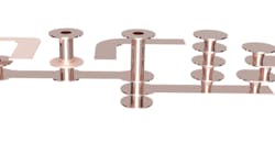
PCB Designers use Vias to electrically and thermally connect parallel layers of copper on a printed circuit board. Vias are made by coating the walls of drilled holes with copper in an electrochemical plating bath. Additional processing can modify the vias for special purposes such as via-in-pad. Take a deep dive into vias in this whitepaper.

