Over the past decades, the high-speed analog-to-digital converter (ADC) performance metric that mattered to most has changed, albeit slowly. Primarily as a result of signal acquisition systems’ ever increasing and insatiable bandwidth requirements, the way in which ADC performance is measured also has changed.
This file type includes high resolution graphics and schematics when applicable.
In the 1980s, we judged an ADC largely on its dc specifications such as differential and integral non-linearity (DNL and INL). In the 1990s, we primarily judged an ADC on its signal-to-noise ratio (SNR). While spurious free dynamic range (SFDR) is also a very important ADC parameter, noise spectral density (NSD) is yet another comprehensive specification that today’s high-speed and gigasample-per-second (GSPS) ADCs can use to define their performance.
Although NSD has been used for a long time to define a converter’s noise, it may be new to many system designers as the headline specification of a new high-speed ADC. NSD could also be a completely foreign concept to some engineers who have focused on other specifications when selecting a high-speed ADC. Below are answers to some typical questions from engineers that help demonstrate why they should learn more about this ADC performance metric.
I have seen the NSD specification on a Nyquist-rate ADC datasheet before, but I never really understood what it meant and why it is important. What is noise spectral density?
NSD has been used for many years as a performance parameter on the front page of many ADC datasheets. You may have noticed that it is a relatively large negative number defined in either dBFS/Hz or dBm/Hz. A typical range that may be observed on a datasheet for an ADC’s NSD could be anywhere from –140 dBFS/Hz to –165 dBFS/Hz. However, this is ultimately defined by the SNR performance of the ADC and the sample rate, as will be described later.
The SNR from an ADC is defined as the log ratio of the signal power to the total non-signal power that is seen at the input to the ADC. Relative to the ADC full scale input, the signal to noise ratio is described as SNRFS. There are several components to the non-signal power, such as quantization noise, thermal noise, and small errors within the ADC design itself. Since the ADC converts a continuous signal into discrete levels using a nonlinear process, quantization noise is inherently created. The quantization noise is the difference between the actual analog input that is typically represented by a sine wave and the value of the smallest discrete step or least significant bit (LSB).
NSD defines the entire noise power, per unit of bandwidth, sampled at an ADC input. For a Nyquist-rate ADC, this noise is spread across the entire Nyquist band, which is equal to half of Fs, the sample frequency, or Fs/2.
What do the units for NSD indicate?
The term dBFS/Hz means that the noise is defined in units of power (dB) relative to the ADC full scale (FS) seen within a frequency bin width of one hertz. One hertz, you might ask? Why so small? One hertz is the baseline unit of noise bandwidth established for how wide of an observation bin, in frequency, that is used to define NSD.
For an absolute reference, the NSD may also be defined by the ADC input power in absolute terms of dBm/Hz. In this case, the absolute full-scale input power for the ADC must either be known or measured based on the input voltage and impedance.
How does the NSD specification help me differentiate ADCs for use in my system?
As the sampling frequency of Nyquist-rate ADCs doubles, the noise density decreases by 3 dB respectively, as it is spread across a wider Nyquist band. For a 2x sample rate, the same amount of input noise power would now be distributed across twice the bandwidth, which increases the SNR. This can be verified by doubling the value of the sample frequency (Fs) in the following formula to realize a –3-dB reduction:
Noise power = 10log10(Fs/2)
As sample rates for high-speed ADCs continue to increase well into the gigahertz range, the benefit of increased SNR due to oversampling can be achieved. When comparing performance metrics for two ADCs, the potential to sample at a higher frequency can be considered with the benefit of a lower noise density.
How is NSD different from the noise floor of my fast Fourier transform (FFT)?
A typical FFT is taken using tens or hundreds of thousands of sample points and perhaps even a few million. For most ADC sample rates, this means that the bin frequency size represents a span of hundreds of hertz or a few kilohertz. An FFT bin size is defined as the Nyquist spectrum (Fs/2) divided by the number of FFT samples, with units of frequency. For example, a 131-Msample/s ADC with a 216 (65.5k) sample FFT has a bin size of:
65.5 MHz/65,5000 samples = 1 kHz per bin
So, the noise of the ADC is spread across the its Nyquist zone in relatively large bin widths that are 1000 times as large compared to the bin width defined within NSD. This includes more noise energy in a single FFT bin.
For the example above, if a very large 65.5-Msample FFT were now to be used for our 131-Msample/s ADC, the bin width would be:
65.5 MHz/65.5 million samples = 1 Hz
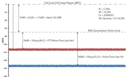
In this case, the noise floor of the FFT would be equal to the noise spectral density of the ADC. But, the total noise power still has never changed. The same noise power is only spread across finer frequency bin widths (Fig. 1).
Contrast this with the NSD definition that has a noise unit of bandwidth, or FFT bin frequency size, of 1 Hz. You can now see why a typical FFT noise floor is almost always higher than that of the noise spectral density. Few engineers use a large enough FFT size in a system to achieve a bin width of only 1 Hz. This is why the noise appears to get lower when the number of samples in an FFT is increased.
However, the total noise is not changing. It is still being spread across the same Nyquist spectrum. Instead of using frequency bin increments that are defined by the sample size, the NSD definition uses smaller frequency bin increments of 1 Hz that capture less noise energy into a single bin.
How is NSD measured and calculated?
For an ideal ADC:
SNR = 6.02*N + 1.76 dB
where N is the resolution of the ADC. This will define the ADC’s quantization noise level. A real ADC will not achieve these performance metrics, as non-linearities from its design will limit its practical SNR to be less than ideal. Seen another way, if we subtract the signal power from the ADC full-scale input power, the rest is just the total noise power. If we summed up all of the 1-Hz bins of noise from our NSD number, we would get a single power noise number equal to the ADC full scale less the signal.
To determine the NSD value for a Nyquist-rate ADC, the calculation of how the noise is spread across a Nyquist zone must be computed and subtracted from the full-scale signal power. To start, we must know the sample rate. Let’s take an ideal 12-bit, 200-Msample/s ADC that has an ideal full-scale SNR = 6.02*12 + 1.76 = 74.04 dB. Its noise is spread across a 100-MHz Nyquist zone (Fs/2). The noise per 1-Hz bin can be calculated using the log function noise power per bin = –10Log10(Fs/2) = –80 dBFS/Hz. For this 12-bit ideal converter, the NSD would be:
–74.04 – 80 = –154.04 dBFS/Hz
Since we live in a non-ideal world with non-ideal ADCs, we must find the ADC’s actual SNRFS. This can either be measured directly or extracted from the manufacturer’s datasheet.
The full-scale input signal power level of the ADC is computed using the known full-scale peak voltage or full-scale RMS voltage and input resistance to the ADC. We can compute the full-scale power in dBm if the input voltage and input impedance are known, where:
Vrms = Vp/√2 or Vp x 0.707
Signal power = ((Vrms2)/Rin) in W
For full-scale signal power in units of dBm:
Signal power = 10 x log(((Vrms2)/RIn) x 1000 mW/W) = 10 x log((Vrms2)/Rin) + 30 dB
What is the shape of an ADC’s quantization noise spectrum? Is it always flat?
Nyquist-rate ADCs operate at the minimum sampling frequency required to capture all of the information about the entire input bandwidth. Most Nyquist-rate ADCs that employ a pipeline, successive approximation register (SAR), or flash type of architecture will have quantization noise that is essentially flat from dc to the Nyquist frequency. As such, they will be “equal opportunity” noise receivers and receive finite power quantization noise equally across the entire Fs/2 spectrum (Fig. 2).
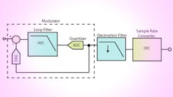
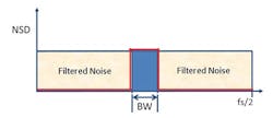
For applications where a full Nyquist bandwidth is not needed, alternate ADC architectures can be implemented. Band-pass continuous-time sigma-delta (CTΣΔ or CTSD) ADCs use a noise shaping function that essentially “pushes” or filters the in-band quantization noise out of the frequency band of interest (Fig. 3). This causes the noise transfer function to have a non-flat shape that is notched lower over a narrow band of interest, smaller than the Nyquist bandwidth. In this band, the CTSD ADC operates to its maximum performance where the SNRFS is the highest (Fig. 4).
Since one of the main benefits of a CTSD architecture is its ability to detect signals within a narrow frequency band, the wideband NSD is not of particular interest. Instead, the dynamic range within the narrow pass band will be highlighted as the performance metric for a CTSD ADC. The noise-shaping transfer function will be determined based on the loop filter order used within the design of the modulator.
How does the processing gain of an ADC affect the noise density and SNR?
There are several applications where the primary signal of interest is located within only a small bandwidth (BW), which is much less than the full Nyquist bandwidth. In this case, digital filtering can be used to filter the noise outside of a smaller bandwidth. This processing can be done using a digital down-conversion stage to decimate, tune, and filter the data before it is output from a Nyquist-rate ADC. Our SNR calculation must then include a correction factor for this filtering that accounts for the processing gain of the filtered noise (Fig. 5):
Ideal SNR (with processing gain) = 6.02*N + 1.76 dB + 10log10(Fs/(2*BW))
Let’s assume we’re using a Nyquist-rate ADC with a sampling frequency of 100 Msamples/s. But, our system application does not need to observe the entire 50-MHz Nyquist bandwidth of the converter. Instead, we only want to observe a smaller one-eighth of Nyquist in a BW section of 6.25 MHz between 20 MHz and 26.25 MHz. If we implement a digital filtering algorithm and tune the filter to this BW of interest, a processing gain of +9 dB due to oversampling can be computed:
Processing gain = 10log10(Fs/(2*BW)) = 10log10(100*106/(2*6.25*106)) = 10log10(8) = 9 dB
For every power of 2 reduction in bandwidth, the processing gain due to the filtered noise will increase by +3 dB. This can be seen in the example above with a 1⁄23 reduction in bandwidth yielding a processing gain of 3 x 3 dB.
What other companion components can impact the NSD performance of an ADC in my system?
Many external factors can degrade the best performance of a high-speed ADC. This can result in a lower SNR and a higher effective noise density. Any complementary component that impacts the SNRFS or sample rate of the ADC can have the potential to impact its NSD in a system. Let’s focus on clock jitter, which is one of the common SNR degradation culprits for high sample frequencies to an ADC.
High-speed, high-resolution ADCs are sensitive to the quality of the clock input. To achieve superior SNR in a high-speed ADC, the root mean square (RMS) clock jitter must be carefully considered, based on the requirements for the application’s input frequency. The RMS clock jitter can potentially limit the SNR of even the best performing ADC, exacerbated at higher input frequencies. While this will not change an ADC’s NSD potential, it will limit its practical SNR performance in a system with a high jitter clock.
As the analog input frequency to the ADC triples using the same RMS clock jitter, the best SNR performance is lowered by 10 dB. The degradation in SNR at a given input frequency (fA) due only to aperture jitter (tJ) can be calculated by:
SNR = 20 × log10[1/(2 × π × fA × tJ)]
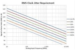
Figure 6 shows the SNR limited performance of various input frequencies across different RMS clock jitter profiles in units of femto-seconds. As the input frequency increases, a lower RMS clock jitter will be needed to achieve the same SNR limit as seen at lower input frequencies. For example, an RMS clock jitter of 200 femtoseconds (fs) limits an ADC’s SNR performance to no better than 70 dB at 250 MHz. But, a 1-GHz input signal would need an RMS clock jitter of 50 femto-seconds or better to achieve the same SNR performance of 70 dB.
The noise spectral density of an ADC can be defined easily as the full-scale signal power of an ADC less the noise power, spread across 1-Hz bandwidth unit increments. A changing FFT sampling depth does not alter an ADC’s spectral noise density. It only spreads the noise across different unit bandwidths of frequency.
This file type includes high resolution graphics and schematics when applicable.
The noise shape can vary depending upon the ADC architecture and whether or not digital filtering is used to filter out-of-band noise. Processing gain can enhance the dynamic range within the bandwidth of interest for Nyquist-rate ADCs that have a far wider bandwidth than a system requires.
Ian Beavers is an applications engineer for the High Speed A/D Converters team at Analog Devices Inc., Greensboro, N.C. He has worked for the company since 1999. He has more than 18 years of experience in the semiconductor industry. Also, he has a bachelor’s degree in electrical engineering from North Carolina State University and an MBA from the University of North Carolina at Greensboro. He is a member of EngineerZone’s High-Speed ADC Support Community. Feel free to send your questions to IanB on Analog Devices EngineerZone Online Technical Support Community.
About the Author
Ian Beavers
Product Engineering Manager, Automation Energy and Sensors, Analog Devices
Ian Beavers is a product engineering manager for the Automation Energy and Sensors Team located at Analog Devices, Greensboro, N.C. He has worked for the company since 1999. Ian has over 20 years of experience in the semiconductor industry. He earned a bachelor’s degree in electrical engineering from North Carolina State University and an M.B.A. from the University of North Carolina at Greensboro.


