Mixed-signal products rarely are created entirely in the analog or digital domain these days. Many new or improved applications are now possible thanks to innovative integration of firmware running on DSPs or micros with analog or mixed-signal silicon analog front ends. Also, many traditionally analog systems now have a firmware component.
These trends mean that analog and firmware designers need to understand the differences between their design disciplines to work together more effectively. Yet analog and firmware designers’ fundamental modes of operation are very different, potentially leading to miscommunication and conflict. Understanding the differences helps to bridge the gap.
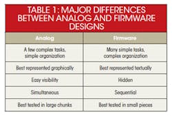
Metaphorically, analog engineering is like getting 10 sharks to jump through a giant flaming hoop, all at the same time, in a brightly lit theater. Firmware engineering is like getting 20,000 piranhas to jump through a tiny flaming hoop, one at a time, in exactly the right sequence, all in a tiny box (table 1). Issues boil down to complexity, test and measurement, and simultaneous versus sequential execution.
Differences In Complexity
Analog engineers spend a good deal of time on layout, grounding, filtering, and circuit design. They need to get that 100-ns response to a 1-mV step. Firmware engineers often aren’t as skilled on these analog issues as their analog counterparts.
On the other hand, when writing system firmware, programmers must frequently deal with difficult logical/sequential puzzles that arise from system states, fault sequences, lists of commands, and interactions between system functions. For example, if A occurs right after B, and the program just started operation C, what should the program do, and what should it communicate to the host system?
Programmers need to work with analog engineers to help solve these problems. However, analog engineers often aren’t as comfortable with these kinds of questions. The key is to understand the importance of these questions and be willing to work through them together.
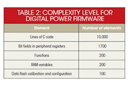
The magnitude of complexity is important in understanding how to deal with it (Table 2). Firmware systems have many more elements than analog designs, but much fewer than modern PC software. In PC programs, modularity and structured programming are vital for managing complexity. In firmware, limited system resources can make modularity very difficult, and less complexity makes it unnecessary.
Limited modularity and resources mean that firmware can be difficult to change. Firmware is changeable and flexible, but the changes and flexibility come at a price. They take time and add more risk. Some parts of the code, like some of the communication interfaces, can be very modular while other parts cannot.
Another key to managing complexity is discipline in naming functions and variables. Analog engineers can help by using clear and consistent signal names, especially for signals that connect to processor pins. The programmer can use the same names inside the program, making the interaction between the program and signals perfectly clear.
Representation Of Content: Text Versus graphics
Analog complexity is best represented graphically while firmware is best represented textually. For analog engineers the basic tool is a schematic. The basic tool of firmware engineers is a written program. In a system the difference is clearest at the processor pins. For the analog designer, the schematic shows it all. Firmware engineers want a signal list showing:
- Signal function
- Input, output, bidirectional
- For analog signals, properties like scaling and bandwidth.
These factors may be obvious to the board designer, but can be unclear for a firmware engineer.
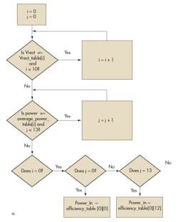
Most analog engineers believe that flowcharts are the best way to represent programs. While early programmers used flowcharts, they are inefficient and take lots of time and effort to make. They also lead to bad programming habits. Flowcharts lead to code that often winds continuously around and becomes very confusing—hence the term “spaghetti” code.
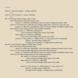
Flowcharts are compatible with first-generation languages like assembly and Fortran. In the 1970s, increasingly complex programs drove people to use ALGOL-based languages, like C and Pascal. Their improved control structures could not be represented well by flowcharts. Thus, pseudo-code was developed (Fig. 1).
Modern firmware complexity is a good match for pseudo-code representation. Learning and using pseudo-code is a great way to understand some of the firmware culture. Once you learn how to write it, it’s a lot easier and faster than drawing a flowchart (Fig 2). Pseudo-code is easy to write for those familiar with the basics of modern programming languages. It’s a very important part of firmware design. Learning it will help you to understand the firmware culture.
Test And Measurement (Visible Versus Hidden)
Analog signals are easy to access for testing and debugging. They are on a copper trace right on the PC board. In firmware, everything is hidden in the processor, thus, executed “inside the box.”
The in-circuit emulator is the most commonly used tool for software debugging. It brings the inside of the processor to the screen of your PC. You can examine and modify registers and memory, single step through the program, set breakpoints to stop the program when it executes specific instructions, and so on. The emulator, however, is of little use in debugging mixed-signal systems like power supplies. It’s best at finding simple logic errors in programs, which are not the big issue with mixed-signal systems.
While problems encountered with a mixed-signal system are different, they tend to fall into two classes:
- Implementing a traditional analog function, like a filter, in firmware or in a blend of digital hardware and firmware
- Matching timing and internal signals to external analog functions.
In both cases, it’s best to use a debugging technique that predates in-circuit emulators—instrumenting code, which means modifying the code to send information outside the box. Instrumentation can be textual or analog. Textual instrumentation is best for testing filters or other programs that transform digital data.
Many evaluation modules (EVMs) have an RS-232 port that can be used with a simple terminal emulator. To perform this kind of testing, send in a pre-calculated set of input data and compare the output to that of a verified model of the function. Textual debugging also can be used for the reporting and control of system functions.
This technique only works if pins are available to send the data. Often there are unused serial port pins on a chip. Even a tiny test pad that can connect to it for debugging is enough. Sometimes there’s a communication bus that can be borrowed for the function.
There are also analog techniques for testing firmware in the system. For mixed-signal systems, they involve meeting the analog designer halfway and putting out signals for an oscilloscope. The simplest technique is toggling an I/O line.
This is a very powerful technique. It’s useful for measuring firmware timing and for telling how often a specific piece of code is executed. Also, it’s very powerful for showing when the firmware has detected a specific event, such as something that the code is normally detecting, like a fault.
It’s also possible to add code to detect a specific event. This I/O line transition can be used to trigger an oscilloscope, or it can be used with other triggers to see how well the program is detecting events, or as a sophisticated trigger generator for looking at a specific analog event. Again, it can only be used if a pin is available.
Another tool can meet the analog designer more than halfway, getting digital firmware to output an analog representation of an internal value. This is possible because often there is a spare pulse-width modulator (PWM) or a digital-to-analog converter (DAC) pin available.
To use this technique, the firmware puts an internal signal out on the pin. With a simple low-pass filter, this signal can be turned into a continuous waveform that can be observed on the scope at the same time as the analog signals for the rest of the system.
When debugging an initial ac-dc power-supply design, we had about 10 or 20 different internal “signals” instrumented at different times. The first step was to verify that the signals were getting through the ADCs cleanly. The next step was to watch the signal go through the internal filters and come out on the other side.
If you have a digital proportional, integral, derivative (PID), you can look at the output of each term. You can look at the error input to the PID. If real detail is needed at a specific time, it’s possible to look at the pulse width directly. This gives the exact value at this point.
These techniques are indispensable in the design of mixed-signal systems and as analog and firmware engineers spend more time together. The general awareness of such techniques will lead to faster and more efficient designs.
Sometimes it may be worthwhile to complete an initial prototyping with a bigger version of the chip, one with more pins for more instrumentation, and maybe a bigger version of the board with test points and built-in filters for the extra PWM pins. In any case, try to squeeze in little test pads for the serial port, a digital line, and a PWM, or more if you can. Everyone will be glad you did!
Firmware engineering works the other way as well. Even though the analog signals are on the outside, visible to anyone watching, the program only knows about them if they are hooked up to a pin. For instance, if there is a hardware over-voltage protection (OVP) circuit outside the processor that provides redundant protection, consider running a signal to let the processor know if it’s been triggered. Otherwise the program will keep trying to run the power supply. If there is a host interface, it may not report the power supply state correctly.
Simultaneous Versus Sequential
Another difference is simultaneity versus sequence. In an analog system, things tend to run simultaneously. In a firmware system, instructions are executed sequentially. Sometimes, the implications are not always clear to analog designers. Frequently, the request is to “Just do this at the end of each switching period.” The answer usually is, “It probably can be done, but….” There are two issues.
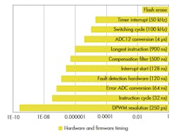
First, only a few things can be done that frequently. Texas Instruments’ ARM-based digital power parts have an instruction clock of about 32 MHz. So for a 200-kHz switching rate, only 160 instruction cycles are available. Some instructions can execute in one cycle, while others can take up to 28 cycles (Fig. 2). Lots of them take two or three or four cycles. Then the whole program execution has to fit into those 160 cycles. If you dedicate 150 cycles to the end of the period, you now have only a 2-MHz processor for everything else, which may not be enough.
Second, it is difficult for firmware to do things at an exact time. There is an end of the switching period interrupt, but there is always a four-instruction-cycle overhead for entering the interrupt. Also, you can’t enter the interrupt in the middle of an instruction. So if the interrupt occurs at the end of an instruction, it takes about 130 ns (four cycles) to start. If the interrupt occurs at the start of that 28-cycle instruction, it takes about a microsecond. The timing of the interrupt, then, may not be very precise.
The ARM-based system has a slower processor with sophisticated peripherals specifically designed to do things at the end of the cycle, relieving the firmware of this duty. A DSP-based system may have a faster processor that can respond quicker, but the same basic issues are still present. This causes the DSP to be busier, since it won’t have as many peripherals to carry the load for filtering, fault detection, and fault handling.
Optimizing the allocation of processor bandwidth is a complex and arcane art practiced mainly by firmware engineers. Software authors don’t worry about it as much, since they have much more bandwidth and much less of a real-time imperative. If it takes a while for a spreadsheet program to sort things out, there’s no real problem. But if a power-supply control takes too long to sort out a fault, equipment could be damaged.
System Components: Testing Big Versus Small Pieces
The final difference is the different nature of system development. The task of getting a system working is very different for an analog versus a firmware designer. With an analog design, generally there are a few very difficult tasks that often are interdependent. So the system is brought up in only a few steps, though each step is complex and may take a long time.
In a firmware system the opposite is true. There are many simple tasks. You can start with just one piranha jumping through the hoop. Then you can add a few more. You can develop little parts and then start to hook them together. In fact, if you don’t do things this way, you are almost guaranteed to fail. Mistakes are inevitable in a system as complex as this. But if you deal with them a bit at a time, they are quite manageable.
Because of the way analog engineers have had to work, they expect the firmware to be ready to go when the board is ready. After all, their analog part is all ready. Firmware engineers try to meet this requirement, but the only way to do it successfully is to use clever testing and emulation techniques to bring the firmware up without the analog components.
It’s useful if it can be done, but it takes a lot of resources. It’s much easier to bring both the analog system and the firmware up gradually together. An added benefit is that the analog portion of the system can be brought up in smaller pieces. Here is a sequence that can be used to bring up a power supply:
- Start the processor running with communication for debugging.
- Verify switching waveforms with no power connected. Make sure the waveforms are right and won’t damage the power supply.
- Bring up switching waveforms with a low voltage and a light load to test output stages. This is done open-loop, so the feedback doesn’t have to work yet.
- Gradually increase the power until it reaches full power, still open-loop, but monitor the loop input to the chip. Also, monitor the other signals from the analog hardware to check for correct function and noise levels.
- Connect (digitally inside the chip) the protection signals, and verify that the protection logic works.
- Finally, enable the feedback loop with conservative coefficients so it won’t oscillate. This is done with slow changes to load and input voltage—no transients yet.
- Then optimize the loop coefficients, subject the power supply to transients and difficult corner cases as well as noise and temperature excursions, and so on.
About the Author
Ian Bower
Ian is a Firmware Engineer with Texas Instruments. He holds a Bachelor of Science - Engineering from the Illinois Institute of Technology.

