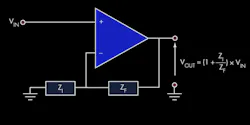
Download this article in .PDF format
Though sometimes taken for granted, designers shouldn’t overlook the intricacies of voltage- and current-feedback op amps—integral players in the analog and mixed-signal worlds. Op amps amplify tiny signals from sensors so analog-to-digital converters (ADCs) can digitize them. They also make it possible to craft active filters with better characteristics than filters built of just coils and capacitors. Although an IC op amp’s circuitry tends to be subtle and complex, its application principles—at least to a first approximation—are relatively simple.
Defining An Op Amp
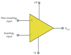
An operational amplifier, or op amp, generally comprises a differential-input stage with high input impedance, an intermediate-gain stage, and a push-pull output stage with a low output impedance (no greater than 100 Ω) (Fig. 1).
Open-loop voltage gain runs very high, on the order of 1 million. The differential input stage implies an inverting and a non-inverting input. With dual (positive and negative) power supplies, it can handle input signals that aren’t necessarily referenced to ground.
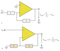
As a practical matter, op amps are always used with negative feedback. That is, the output gets fed back to the inverting input through some impedance. Also, op amps may be optimized for specific applications by emphasizing different performance characteristics (see the table).
Negative Feedback Controls Gain, Frequency-Domain Behavior
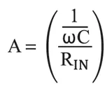
The ratio of output impedance to input impedance determines the gain of an op amp that uses negative feedback (Fig. 2). If one of these impedances is reactive (practically speaking, if it’s a capacitive feedback impedance) and there’s a purely resistive input impedance, gain A is given by:
In this case, the gain characteristic is frequency-dependent. From a frequency-domain standpoint, the circuit represents a low-pass filter. In the time domain, the circuit’s output is the integral of the input signal. Also, the apparent capacitance of the circuit is multiplied. By simply varying the input resistance, it becomes easy to build a circuit with an output voltage that’s 0.1 or 1 or 10 times the integral of the input voltage.
Input Bias/Offset And Common Mode
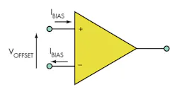
Actual input stages may be subject to bias and offset errors (Fig. 3).Input bias currents (on the order of nanoamperes) flow because the input impedance is finite, and they ultimately affect linearity. Op-amp designers may trade off higher bias currents for higher speeds. Offset represents the voltage difference caused by a variation between bias currents on the two inputs.
Real-world op amps also are limited in their maximum allowable input voltages. Such an allowable common-mode swing generally falls below the supply voltages. Some op amps are designed for rail-to-rail (or nearly rail-to-rail) input voltage swings.
Voltage- And Current-Feedback Op Amps
Practical differences exist between voltage and current-feedback op-amp topologies, both in the way they’re built and how they’re used.
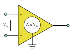
Voltage-feedback (VFB) amps control the output voltage, in effect, by a voltage-gain stage (Fig. 4). The voltage difference between the two inputs is multiplied by a dimensionless gain constant (A). In a VFB amp with negative feedback, the output changes to drive the voltage difference between the inverting and non-inverting input to zero.
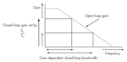
An ideal VFB would possess very large open-circuit gain that’s independent of input frequency. However, in a real-world VFB, the open loop gain is large at dc, but rolls off at 6 dB/octave (Fig. 5). As open-loop gain decreases, the negative-feedback op amp’s gain drops below the ratio RF/RI. When the open-circuit gain equals RF/RI, the circuit’s overall gain will be half its dc value. This is called the −3-dB bandwidth.
For most of the frequency range, the product of gain and bandwidth, or gain-bandwidth product (GBP), becomes constant. Consequently, for any given real-world VFB amplifier, it’s possible to design a circuit with high gain or high bandwidth, but not both.
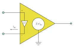
From a topological standpoint, two key factors differentiate current-feedback (CFB) amplifiers from their VFB counterparts. First, a unity-gain buffer sits between the non-inverting input and the inverting input (Fig. 6). The buffer typically has very high input impedance and very low output impedance.
6. CFB amps include a unity-gain buffer across the input. The output voltage is the current that flows between the inputs, multiplied by a transfer impedance.
The buffer affects the CFB’s open-loop characteristics in various ways:
- Very high input impedance on the non-inverting input
- Very low input impedance on the inverting impedance
- Very low output impedance
The second difference is that in a CFB, a transfer function, operating on the current flowing through the buffer between the inputs, basically controls the output voltage. Transfer impedance (Z) multiplies this current.
In a CFB with negative feedback, the signal from the output will attempt to drive the error current to zero. This is otherwise known as “current feedback.”
It’s important to note that CFB amps don’t have the gain-bandwidth limitations of VFB amps. Instead, the CFB amp limits the size of the feedback impedance, which is given as a resistance value in datasheets.
Ideal-case voltage gain in a CFB amp (and in VFB amps) is still set by the ratio of feedback-to-input resistance. But for real-world amplifiers, gain rolls off with increasing frequency. Therefore, the size of the feedback resistor affects frequency response, which ultimately restricts the range of possible RF values.
In practice, CFB amp bandwidth does vary a little with gain, although not as drastically as with VFB op amps. That’s mainly due to the non-zero output impedance of the input buffer, whose effect is to alter the loop gain and, hence, the closed-loop dynamics.
Unlike VFB amplifiers, CFB op amps don’t experience slew-rate limiting. RF alone will govern CFB transient response, as is the case with frequency response. Likewise, it takes very little time (nanoseconds or less) for a CFB amp’s output to settle within 0.1% of its final value.
CFB Limitations
Given their gain-bandwidth advantages, why do engineers continue to design circuits with VFB amplifiers? First, VFBs offer lower noise and better dc performance than CFB op amps. Second, VFB amps can be employed as integrators simply by using a capacitor as the feedback impedance. In contrast, CFB op amps must avoid a direct capacitance between the output and the inverting input. There are workarounds, but they add to the circuit’s complexity.
Op-Amp Characteristics
Voltage-feedback op-amp datasheets specify five different gains: open-loop gain or AVOL (which may be 160 dB or higher without negative feedback), closed-loop gain, signal gain, noise gain, and loop gain.
Loop gain is the difference between the open- and closed-loop gains, or the total gain through the amplifier and back to the input via the feedback network. It comprises signal gain and noise gain. Signal gain is the gain experienced by an input signal, while noise gain reflects the input offset voltage and voltage noise of the op amp at the output.
A datasheet will also reveal various distortion measurements. Total harmonic distortion (THD) and THD+N (THD plus noise) are both measurements of distortion generated by a single-tone sine-wave input. Intermodulation distortion (IMD) is a measurement of dynamic range produced by the interaction of two tones. Third-order intercept point (IP3) measures the effects of third-order IMD.
Other specifications include the 1-dB compression point. It represents the level of input signal at which the output signal is compressed by 1 dB from an ideal input/output transfer function. This defines the end of an amp’s dynamic range.
Signal-to-noise ratio (SNR) also defines the dynamic range. It measures (in dB) the maximum signal level to the rms level of the noise floor.
In RF work, noise factor and noise figure are important specs. Noise factor relates the noise generated by the amplifier to the thermal noise of a 50-Ω resistor at room temperature. Noise figure is noise factor expressed in dB; i.e., 10 × log10 (noise factor).
References:
- Jung, Walt, “Op-Amp History.”
- Maliniak, David, “Online Design Environment Demystifies Op-Amp Puzzles,” Electronic Design, Jan. 19, 2004.
About the Author

Don Tuite
Don Tuite (retired) writes about Analog and Power issues for Electronic Design’s magazine and website. He has a BSEE and an M.S in Technical Communication, and has worked for companies in aerospace, broadcasting, test equipment, semiconductors, publishing, and media relations, focusing on developing insights that link technology, business, and communications. Don is also a ham radio operator (NR7X), private pilot, and motorcycle rider, and he’s not half bad on the 5-string banjo.
Voice Your Opinion!
To join the conversation, and become an exclusive member of Electronic Design, create an account today!

Leaders relevant to this article:
