Added ADC Improves Analog Square-Root Extraction Accuracy
This file type includes high-resolution graphics and schematics when applicable.
Known devices for taking the square root contain an operational amplifier and a multiplier connected in a feedback loop. The accuracy of these devices depends on the method of building the multiplier, with the most accurate using logarithm and anti-logarithm functions. However, even these are not accurate to better than ± 0.1% without trimming or calibration. The circuit proposed here removes this limitation associated with the analog multiplier, by using analog-to-digital conversions to increase the accuracy of the square-root derivation.
The device is based on the ratio:
K2(1 – N)2 = X
where K2 is a constant and X is proportional to VIN, resulting in:
K(1 – N) = √X
and
K(1 – N) = X/K(1 – N)
These ratios are realized in this device by creating two voltages in approximate balance: V1, which is proportional to K(1 – N), and V2, which is proportional to X/K(1 – N). N is constrained as 0 ≤ N < 1.
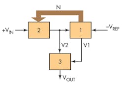
The approach (Fig. 1) consists of three functional parts, where two chains create voltages for subsequent comparison. Part 1 consists of reference voltage VREF, an analog-to-digital converter (ADC) with digital-to-analog converter (DAC), an operational amplifier (op amp), a comparator, and an up/down counter with a control circuit. Part 2 contains an op amp with a DAC connected in feedback, creating the signal of the ADC. Part 3 is a summing amplifier that sums the outputs of Parts 1 and 2 and scales the output voltage proportional to the square root of the input voltage.
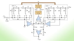
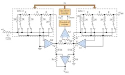
In the example circuit (Fig. 2), the analog part of the device contains amplifiers A1, A2, and A4; the digital-to-analog part consists of DAC1 and DAC2; and the digital part is the up/down counter. This example uses only four switches within each DAC, but the number of switches can be increased to enhance the accuracy.
In Part 1, resistor R1 is connected in feedback to DAC1, and is proportional to R-2R of DAC1: R1 = n1R. The output voltage of A1 is:
V1 = n1VREF(1 – N)
In Part 2, R2 is also proportional to R-2R of DAC2: R2 = n2R. The output voltage of A2 is:
V2 = –[VIN/n2(1 – N)]
The value of (1 – N) is defined by setting all switches in both DAC1 and DAC2 to their initial position and the last resistor in the network as R-2R. The rise of N determines the decrease of voltage gain V1 and the increase of voltage V2. A decrease in N results in the opposite change. Voltages V1 and V2 are compared by comparator A3. The output of A3 is binary with two levels for operating the counter control, which consists of a pulse source and switches for up/down pulse count.
With V1 and V2 in approximate balance, the errors of these voltages are in the range of the least significant bit (LSB) and have opposite polarity, so combining them can achieve a partial correction of the end result. This is done by connecting V1 and V2 to amplifier A4 by two resistor divisors R4/(2n3 × R4), where V1 = V2 = n3√VIN.
In this example, the scale factors have been chosen to keep calculations simple, based on a standard analog range of 0 < VIN ≤ 10v for the input voltages and a VREF = –10v. For the maximum VIN = 10 V, choosing n2 = 1.6 = 4/2.5 allows the choice of K = 4, yielding n1 = 1.0 and n3 = 2.5.
The accuracy of this circuit is limited only by the number of switches in each DAC, with each additional switch representing the next least significant bit in binary. Note that N = z/(zMAX + z0), where z is the current sum of all bits, zMAX is the maximum possible sum, and z0 is the least significant bit. The proposed scheme thus provides a way of increasing the accuracy of square-root derivation beyond that of conventional integrated circuits.
Reference:
Electronic Circuits Handbook for Design and Application, Tietze, Ulrich, Christoph Schenk, & Eberhard Gamm. 2nd ed., Springer 2008.
About the Author
Yakov Velikson
Electronics Engineer
Yakov Velikson retired from Kerfott Guidance & Navigation Corp. He holds a PhD in electrical engineering from St. Petersburg Electrotechnical University and is the author of 45 patents in the areas of analog-to-digital and digital-to-analog processing.


