This file type includes high-resolution graphics and schematics when applicable.
Back in 2011, National Semiconductor CTO Dennis Monticelli sent Bob Pease a note linking to some low-voltage vacuum tubes. Bob copied me on his response:
“Naw, I never ran into these 12-volt tubes before. Wild business. I guess designing with them would not be much weirder than designing with germanium transistors. I have done a little designing with geranium transistors, NPNs and PNPs. So I do know a little about them. I did make a good design for a voltage-to-frequency converter [VFC] that was ultra-linear (0.01%) 36 years ago. I designed it to bias up its silicon transistors so nicely that when I took it to +205 degrees C, and the transistors began to leak and look like germaniums, the circuit still worked well. In other words, this was a circuit that would run with geraniums up to 55 degrees, or silicon up to 205, because they look about the same, leaky and low Vbe [base-emitter voltage]. This is like Bob Widlar's LM12, where the silicon gets up to 260 degrees C, and still works like a transistor (well, a hot transistor). That VFC was a good challenge. But our customers did not materialize. Sometimes, guys who say they really need something dry up and blow away when you give them what they ask for...... (Ahem.) / beastly. / rap”
Pease wrote his first V-to-F article in Electronic Design back in 1993. In 1994, he followed up with two more, "What's All This V-F Converter Stuff, Anyhow, Part 1," and "Part 2." Pease mentions those last two articles were taken from his chapter in Jim Williams’ book, Analog Circuit Design: Art, Science, and Personalities.
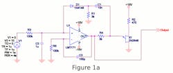
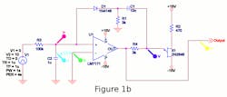
The Part 1 article started out with a circuit that Pease heard of in 1967. A Swedish design team had come up with a V-to-F converter that used a unijunction transistor (UJT). Pease remembered the circuit with a negative feedback network (Fig. 1a). After experimenting with the circuit in OrCAD Capture/PSpice 9, I had better luck removing the negative feedback network and connecting the transistor to –15 V (Fig. 1b).
The unijunction transistor is nearly obsolete, but you can still get the 2N2646 at Newark for $3.25 (2016). Mouser lists them as obsolete and Digi-Key only has programmable unijunction transistors that are still used to trigger SCRs and TRIACs in ac circuits. Hobbyists love UJTs, since you can make an oscillator with three resistors and a capacitor.
What looks like a base connection on the UJT is really the emitter. When you increase the voltage on the emitter, is presents a fixed resistance between the emitter and base-1. When the input voltage on the emitter reaches a threshold, the resistance between the emitter and base collapses to a lower resistance. If you rig things so that this collapsing resistance also lowers the input voltage to the emitter, then the UJT resets and goes back to the higher resistance. Oscillations ensue.
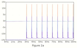
This circuit is insensitive to the input offset of the amplifier. If the offset drives the output high, the UJT will trigger and draw enough charge out of the input capacitor so that the output goes low, and then the circuit operates normally. If the input offset of the amplifier drives the output low, sooner or later the input voltage will charge the capacitor enough so that the output goes positive (Fig. 2a).
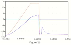
2. The UJT V-to-F converter takes a while to start when the offset voltage drives the output initially low (a). Once it runs, the UJT creates a negative pulse (b). Input capacitor reset is 2 µs (teal x100).
Like the other circuits Pease goes on to describe, only the reset capacitor C1 needs to be precise over temperature. When the circuit switches, the diode steers charge out of the input capacitor C2. The charge is the voltage across C1 times its value. The voltage across the capacitor swings from the trigger point of the UJT to close to −15 V (Fig. 2b). The little “hook” in the UJT emitter voltage (blue) looks terrible, but it does not draw any charge out of the input cap (teal x100), so it does not matter.
The fundamental problem with all three circuits described by Pease is that when you have to take a fixed time to reset or discharge that input capacitor C2, you’re putting in an inherent nonlinearity in the output. Jim Williams describes this in the sidebar at the end of his classic Linear Technology application note AN14 (pdf).
Now Pease maintains the range of the Swedish circuit was only 1 kHz. The UJT in my Spice simulation takes 2 µs to reset the input capacitor. So at 1 kHz, that 2-µS “lost time” to the integration represents 0.2%. I can hear Pease screaming “Spice lies,” and in a way he is right. My simulation does not account for temperature drift and it relies on a UJT model that may not be accurate. Furthermore, in production, the trip point of various different parts may cause real headaches.
To me it’s not so much that Spice lies, but it represents the mathematical operation of a circuit. Spice is not sufficient to fully understand a circuit, but I think Spice is a great way to begin to understand the operation of the circuit.
The improved circuit that Pease describes in Part 1 (Fig. 3) dispenses with the vagaries of a trigger point in a UJT. He uses an amplifier as a comparator to make an oscillator. When you try to understand an op-amp circuit, you assume the plus and minus pins are at the same voltage. When trying to understand a comparator circuit, you assume the plus and minus pins are never at the same voltage. If they are, then noise makes the output chatter in some indeterminate manner.
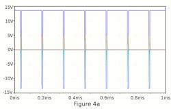
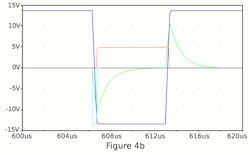
Pease used positive feedback to ensure that the inputs pins don’t dither or noise won’t chatter the output (Fig. 4a). The tiny 22-pF C3 pulls down the plus pin momentarily, so that the amplifier slews all the way negative. Once that swing completes, the positive feedback has done its job, and now works in the other sense, as the amplifier slews positive (Fig. 4b). Think of it as an ac hysteresis.
4. Peaseâs first stab at a V-to-F converter switches cleanly and works up to 10 kHz (a, blue). The output slews rail-to-rail (blue) and the current pulse out of the input capacitor is 500 ns (b, teal x100).
A V-to-F made in this manner creates new problems, though. First off, the slew rate of the amplifier determines the reset time. With a TL031 JFET amp, the simulation showed the reset time to be 6 µs, three times worse inherent nonlinearity than the UJT circuit. When I put an LM7171 amplifier in the circuit, the reset time went to 500 ns—four times better than the UJT.
Unfortunately, this circuit has a serious drawback. If the offset voltage of the particular part makes the output go low, then the input capacitor C2 charging up the minus pin of the amplifier will have no effect. It just makes the amplifier stick at the bottom rail a little harder. I lucked out in my Spice simulations. The model of the TL031 and LM7171 both drove the output high. After the input cap charges up, the output drives low, pulls charge from the input cap, and the circuit will work as intended.
In the circuit of Fig. 3, Pease uses the input resistor values to try and ensure that the circuit will start up. The amplifier he used has NPN inputs, which means the bias currents flow into the input pins. Pease made the minus pin input resistor 25k and the plus pin resistor 22k. This will bias the minus pin a little below the plus pin, so the output will switch when C2 starts charging up. This little bias has to be greater than any offset voltage in any part that gets used in production.
It’s a bit risky to count on the input bias current to wash out any offset voltage. It would get you in real trouble with modern amps that have input bias cancellation. No matter whether PNP or NPN inputs, the bias currents are trimmed in manufacturing (pdf). Sometimes they flow out of the pin, sometimes in.
Pease improved the circuit by using a NPN transistor in the feedback. This decouples the tiny change of the voltage on the input capacitor from the charge-shuttling capacitor C1. The voltage across C1 is now between a grounded base-emitter junction and output swing of the amplifier. This brings up another problem with the circuit—its dependence on the power supply. This is why some analog engineers power a circuit like this from a voltage reference.
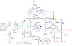
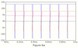
Pease addressed the offset problem in his 1974 production circuit, the Philbrick 4701 V-to-F converter (pdf) (Fig 5). He added a startup network with Q3, R12, R13, and C5. If the amplifier output floats to the negative rail due to offset voltage, it turns on the PNP, which pulls the minus pin to –15 V below the plus pin. This drives the amp output positive. Then as the input capacitor is charged by the input voltage, the amp goes negative and the circuit can continue to work. Since the output of the working circuit is short negative pulses, the average voltage at the Q3’s base is a few volts and it never turns on while the circuit is operating properly (Fig. 6a).
Pease made two other improvements. He clamps the output of the amplifier with a Zener inside a diode bridge. He picked a Zener that has a little temperature coefficient, although the diodes will still have a negative tempco. As he explained in Part 2, this is intentional. At higher temperature, the diode voltages drop and the voltage swing increases a bit. Pease used this to offset other temperature coefficients in the circuit.
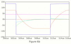
6. In Peaseâs 4701 V-to-F converter, the output is clamped by a Zener bridge (a, yellow). The startup voltage never goes negative when the circuit is operating (purple). Capacitor C6 does draw current out of the input capacitor for 8 µS (b, teal x100). C6 also rounds off the clamped output (b, yellow).
The other improvement is what he referenced in the quote at the beginning of the article. Instead of a single transistor with a diode clamp, Pease biases two diodes (D1 and D2) by pulling them up with a 150-k⦠resistor. Then he connects the feedback network to the top diode with D3. Now the feedback network is biased up a diode drop from ground, which matches the base-emitter diode drop of the transistor. This keeps the transistor on the edge of conduction. Better yet, the diode drops all change together over temperature; therefore, at a high temperature, the transistor is still on the edge of conduction.
This is what Pease bragged about in his email—the leakages that show up at high temperature are canceled out. Unlike the patent application Pease refers to, this circuit connects the positive feedback network to the amplifier directly, instead of to the Zener clamp circuit. The positive feedback network will not affect the precise clamped swing Pease used for the charge transfer.
Pease said he added C6 to the negative feedback network so that “the amplifier wouldn't balk.” The problem is it increased the reset time to 1 µs (Fig. 6b). Perhaps the reduction in charge that C6 pulls out of input capacitor C1 is then offset by the addition of charge when the amp slews the other way. So even though the effective reset time may be still a couple of microseconds, it’s the net transfer of charge by C2 that matters. This is why Pease stresses that C2 be polypropylene.
Pease got exasperated with engineers that thought their job was done after a Spice simulation. It’s obvious that he incorporates many little tweaks that compensate for temperature change and the inherent nonlinearity of a fixed reset time.
While I understood Pease when he shouted “Spice lies!,” I also think Spice can teach us a lot about circuits. I know some of the latest Spice models of amplifiers are very good. They model noise, and current in the supply pins, and the behavior of the amp as it comes out of saturation when the output hits the power-supply rails.
To go at this circuit again, I would get those good models and use LTSpice. Another good alternative is MultiSim. They do their own models to their own consistent standards. A problem with my simulation is that the older parts had much poorer models. I learned to reduce step size to 10 ns if I wanted an accurate result.
Another trick would be to use a fast comparator chip that’s meant to swing to the rails. Some op amps have diode clamps across the input pins and might not work right as a comparator. Pease used D8 and D9 in his 4701 to make up for shortcomings in the LM301 amplifier. If a Zener bridge compensates for inherent nonlinearity, then we should use it. Otherwise, maybe running a comparator off a precise power-supply voltage will give adequate linearity.
In analog, adequate is a key concept. If a simple goofy circuit with a UJT does the job you need it to, than great. Do realize that Spice will not tell you anything about part-to-part variations over your manufacturing run, or all of the temperature problems, unless the models have temperature built into them by you or the model provider.
I see Pease’s point. Spice is Platonic, the mathematical ivory-tower theory of how the circuit should work. A soldering iron is Aristotelian, the reality-based A-is-A fact of actual hardware. I think we need both, like the scientific method, to get the best results.


