Adopting AI-Based Circuit Optimization and Migration
What you’ll learn:
- Why has analog design been a manual process?
- How artificial intelligence is improving the EDA process.
The use of artificial intelligence (AI) has gained significant traction in many domains of EDA, and for good reason. AI learns from experience, adapts, and converges on a solution while considering conflicting goals with complex tradeoffs.
Such characteristics make AI highly valuable in tackling many of EDA’s hardest challenges, where traditional optimization approaches—either manual or algorithmic—are either sub-optimal, too slow, or fail altogether. AI has the potential to revolutionize the way we design, optimize, and, in particular, migrate analog designs.
Traditional Optimization Approaches Fall Short
Advances in EDA algorithms have made it possible to scale digital chips to the size of billions of transistors. The scaling of digital design automation builds on abstractions of digital signal levels (1s and 0s) and synchronous operation (discrete time), allowing for a divide-and-conquer approach.
Analog design, on the other hand, doesn’t benefit from such abstractions. Individual elements of the design influence each other in complex interactions, making it impossible to optimize one part of the circuit without affecting others. Also, the design metrics are complex, as designers need to consider dozens of metrics, such as supply current, signal-to-noise ratio, jitter, hysteresis, slew rate, CMRR, DC gain, and more across hundreds of process corners.
Due to these inherent complexities, analog design has remained a largely manual process. This puts severe limits on the potential to exploit the multitude of specialized sub-nodes made available from foundries to take advantage of market opportunities. To understand why this is so, let’s look at where traditional optimization approaches fall short.
The purpose of optimization is, in essence, to deduce circuit characteristics (e.g., transistor sizes, layout placement, routing topology, etc.) that fulfill a desired outcome in terms of circuit behavior or performance (i.e., power consumption, noise margin, signal duty cycle, slew rate, etc.).
If the desired outcome can be modeled in a simple manner, with a model that’s at least rank order correct, then a traditional optimization algorithm can be created. This has been done successfully in many of the individual steps of the digital implementation flow, leading to a highly automated optimization process.
For example, digital circuit performance can be modeled because circuit behavior is able to be simplified to timing delays—that is, optimization of static timing delays is essentially a linear problem. Analog circuits contain much more complex behavior. They build on nonlinear device models, with no simple proxy function.
Physically accurate models of analog circuits will simulate the exact behavior across all metrics, given the detailed circuit topology and parameters. However, due to the complexity of the underlying models, and of the interactions between the various elements in a design, even the simulation itself is an iteratively converging process. There’s no sufficiently accurate, simplified way to emulate the outcome, and no way to move backwards from desired outcome to circuit characteristics.
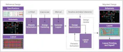
Hence, analog design optimization has remained a largely manual process, which requires advanced designer expertise, time, and patience. Figure 1 illustrates how the optimization step is a manually intensive and key step in a traditional analog design flow for migrating an analog design.
AI-Based Analog Optimization
AI-based approaches do well in addressing optimization problems where traditional algorithmic approaches fall short. AI holds the potential to automate the manual loops in the design process. Much like a human designer, AI performs and learns from experiments, combining learnings across each of the experiments to understand and navigate in the solution space. In general terms, this approach is called sample-based optimization.
Sample-based approaches such as grid search, i.e., parameter sweeping, and random search, i.e., Monte Carlo simulation, have traditionally been used to aid designers during the analog design process. However, these approaches don’t scale well. The number of samples required for sufficient solution space coverage scales exponentially with design complexity.
More efficient general methods do exist, such as Bayesian Optimization, which is widely used in machine-learning applications. A Bayesian Optimizer builds a probability model of the objective function and uses it to select new sample points with high probability of scoring well in the metric space. As such, it takes learnings from previous samples to build a model that helps select future samples.
An AI-based approach represents an even more focused, intelligently directed way to navigate a large and complex solution space to find sample points that meet the specification. An AI capability can be devised as a sample-based optimization system that dynamically learns about the problem it’s tasked to solve.
Such an AI approach can use actual, multi-corner/multi-testbench simulations to drive exploration of complex corner and testbench dependencies. It can dynamically navigate process corners to reduce the number of simulations required, while converging across all corners. Through this process, the AI tool learns from its simulation experiments, using a live feedback loop to converge toward a solution that meets the specification.
A key advantage of such an AI system is that it doesn’t depend on any specific form of the problem it’s optimizing. However, unlike less efficient sample-based approaches, it will more efficiently self-adapt to the underlying objective. It also doesn’t optimize a proxy, but rather is driven by the actual circuit simulation.
Such a system is possible because the AI system makes informed decisions based on the experiments that it runs, reinforcing its internal perspective of the problem and objectives, which enables fast convergence.
AI-Based Analog Migration
Macro trends, including the slowing of Moore’s Law, manufacturing capacity constraints, and a challenging geo-political climate, are driving the need for newer capabilities to rapidly move designs between process nodes.
To take advantage of market opportunities and be resilient to supply-chain challenges, it’s essential for semiconductor companies to maneuver the supply-chain landscape with agility, including porting products from one foundry to another and from one technology node to another. While AI can help accelerate and automate circuit optimization in general, it holds a particular advantage during design migration.
As illustrated in Figure 1, the analog design migration process starts with a reference design, with specification, schematic, and layout in a given technology node, and ends with a completed and functional layout in the target node. The challenge of migrating an analog circuit from one node to another differs from general analog circuit design, in that the circuits are based on a prior version of the design.
This is good news for AI: Any design that’s been optimized in one context holds valuable learnings which are useful, even if the context, such as the technology node, has changed.
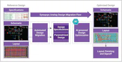
Figure 2 illustrates an AI-driven, automated design migration process. The first step is to migrate to the target node. Circuit elements and transistors are mapped to equivalent elements in the target node, the specification is adapted to the target, and the design is parametrized with parameters required to adjust the circuit to the specifications.
After the basic migration to the target node, the circuit typically isn’t functioning according to the specification. The migration process has moved it off center. The next step is for the AI-driven optimizer to tune the design parameters to recenter the circuit to meet the specification in the target node.
In addition to recentering a schematic, AI can be used to recenter a circuit as it moves through the design phases, from schematic optimization to layout and ECO. The AI doesn’t have to start from scratch at each stage. When adding estimated layout parasitics, the design will be off again and needs recentering, which the AI can do. This can also be handled at the final stages of optimizing with extracted layout parasitics in the optimization loop.
Used properly, AI can significantly accelerate the design process, with fast recentering of a new or incremental design version, the same design in a different technology node, or at later stages of the design process.
How EDA Algorithms Are Enhanced Using AI Optimization
As advances in EDA algorithms have enabled tremendous scaling of digital design complexity and designer productivity, via optimization algorithms, analog design has remained a largely manual process. This is due to the complexity of the circuit functionality and characteristics together with limitations of traditional optimization approaches. It places limitations on the potential for design companies to quickly take advantage of market opportunities.
The use of AI has gained significant traction across EDA. In turn, AI-based optimization has emerged as necessary to address the complexity of the analog design challenge.
As mentioned, AI-based circuit optimization uses actual, multi-corner/multi-testbench simulations to drive exploration of complex corner and testbench dependencies. It learns from its simulation experiments, using a live feedback loop to converge toward solutions. Thus, it’s ideally suited to automate the analog circuit design process.
While AI offers clear value during optimization in general, it also enables advanced new use-models. Recentering during node-migration of analog circuits is fast, as the learnings from the prior design implementation can be retained and exploited. Similarly, AI can quickly recenter a design as it moves through the design process, from schematic to layout and ECO.
About the Author
Tobias Bjerregaard
Sr. Director of AI, Synopsys EDA Group
Tobias Bjerregaard is Senior Director of AI for the Synopsys EDA Group.
Voice Your Opinion!
To join the conversation, and become an exclusive member of Electronic Design, create an account today!

Leaders relevant to this article:


