Tiny Non-Reflective RF Switch Pushes to 50 GHz
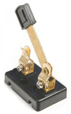
The single-pole, single-throw (SPST) switch has been a necessity since the earliest days of electricity and with good reason: It has many simply described yet vital roles in circuits spanning DC up into the highest ends of electromagnetic spectrum. While the classic knife switch provides a well-defined function and is still widely available and in use (Fig. 1), it clearly is inadequate to meet the needs today’s wired gigahertz-plus circuits due to its large size, modest bandwidth, and very slow switching speed.
Read more for electronica 2024
While mechanical switches can operate into the tens of gigahertz with impressive specifications—they’re marvels of electromechanical and RF design—the strong trend is toward solid-state switches. This is especially the case when signal power levels are low to moderate due to their reliability, size, switching speed, and design-in compatibility, as long as they have the needed bandwidth, of course.
ADI’s New Gigahertz-Class Analog-RF Switches
Echoing that trend is a recently introduced trio of similar silicon-based, gigahertz-class, non-reflective analog-RF switches from Analog Devices: the ADRF5010 (100 MHz to 55 GHz); ADRF5030 (100 MHz to 20 GHz); and ADRF5031 (9 kHz to 20 GHz).
[Ed. Note: If you are unfamiliar about the difference between non-reflective (also called absorptive) and reflective switches, their designations emphasize their difference: Non-reflective switches use a 50-Ω load termination in each output port, which results in a low VSWR, as the port’s terminating resistance absorbs the incident signal energy that would otherwise reflect from an unterminated port. These switches are used where it’s important to minimize reflections back to the RF source. In comparison, reflective switches have no termination resistors, so their open ports have a lower insertion loss. Reflective switches go into applications where high off-port VSWR isn’t critical, and the required impedance match is provided at another point in the system.]
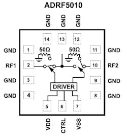
For the ADRF5010, the highest-bandwidth device in the trio (Fig. 2), target applications are the expected areas of test and instrumentation; cellular infrastructure including 5G/mmWave installations; military radios, radars, and electronic countermeasures (ECM); microwave radios and very small aperture terminals (VSATs); and industrial scanners.
The ADRF5010 operates from 0.1 to 55 GHz with insertion loss less than 2 dB and isolation greater 28 dB. Through internal drivers, it features CMOS- and LVTTL-compatible control with RF switching time of 30 ns, while RF settling time is 50 ns to 0.1 dB of final RF output. Input linearity is better than 33 dBm typical (P0.1dB) and input IP3 is greater than 60 dBm (typical).
How the ADRF5010 Switch Handles Power
Power handling is often an issue with solid-state switches. For the ADRF5010, it’s characterized for the three modes of through-path, terminated path, and hot switching, under the three conditions of peak power, pulse, and continuous (CW) power for each. For through-path, the corresponding power ratings are 36, 33, and 30 dBm; for both the terminated and CW paths, they are 33, 33, and 30 dBm, all respectively.
The ADRF5010 requires dual supply voltages of ±3.3 V and can operate with a single positive supply voltage (VDD) while the negative supply voltage (VSS) is tied to ground. In this operating condition, the small-signal performance is maintained, and the switching characteristics, linearity, and power-handling performance are derated.
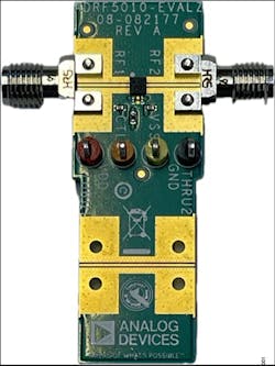
The ADRF5010 comes in a 14-lead, 2.25- × 2.25-mm, land-grid-array (LGA) package and can operate from −40 to +105°C. Even a basic function such as a switch with its simple I/O, but operating at these frequencies, needs support beyond its datasheet. The EVAL-ADRF5010 Evaluation Board fulfills this critical role (Fig. 3). The board package includes a detailed User Guide defining test setup, PCB layout, schematic, bill of materials (BOM), and more.
Despite the apparent similarities among the three switches, they don’t share a unified datasheet. Instead, each gets its own attention via an individual landing page:
Each of the landing pages calls out links to respective datasheet, evaluation board, user guide, and more.
Read more from electronica
About the Author

Bill Schweber
Contributing Editor
Bill Schweber is an electronics engineer who has written three textbooks on electronic communications systems, as well as hundreds of technical articles, opinion columns, and product features. In past roles, he worked as a technical website manager for multiple topic-specific sites for EE Times, as well as both the Executive Editor and Analog Editor at EDN.
At Analog Devices Inc., Bill was in marketing communications (public relations). As a result, he has been on both sides of the technical PR function, presenting company products, stories, and messages to the media and also as the recipient of these.
Prior to the MarCom role at Analog, Bill was associate editor of their respected technical journal and worked in their product marketing and applications engineering groups. Before those roles, he was at Instron Corp., doing hands-on analog- and power-circuit design and systems integration for materials-testing machine controls.
Bill has an MSEE (Univ. of Mass) and BSEE (Columbia Univ.), is a Registered Professional Engineer, and holds an Advanced Class amateur radio license. He has also planned, written, and presented online courses on a variety of engineering topics, including MOSFET basics, ADC selection, and driving LEDs.


