Tailoring the Design of Transimpedance Amplifiers to Infrared Sensor Apps (Part 2)
What you’ll learn:
- How transimpedance amplifiers are used in fiber-optic communications.
- Application-specific design and topology considerations for TIAs.
For Part 1, click here.
High-speed optical communications applications have some high-level transimpedance-amplifier (TIA) circuit similarities with laser rangefinders (LRFs) and LiDAR. However, there are also many differences, especially at the product implementation level.
While LRFs and LiDAR generally require high linearity across the input dynamic range, a TIA designed for high-speed communications must amplify the incoming photocurrent and determine if a one or zero has been received to output the appropriate quantized digital value. Another major difference involves the bandwidths needed to support data rates of many gigabits and beyond, typically between 1 GHz and 40 GHz+, while still supporting transimpedance gains of many kilohms.
Therefore, TIA stability and self-oscillation become key design considerations. The tiniest excess parasitic capacitance and inductance at the TIA input can result in self-oscillation and reduce optical input sensitivity due to increased front-end noise.
Signal overshoot, peaking, and ringing must all be critically controlled to maintain sensitivity and meet the required bit error rate (BER). The length, angle, and thickness of the bond-wire connection between the avalanche photodiode (APD) and TIA and other TIA bond-wire connections must be carefully controlled to avoid stability issues.
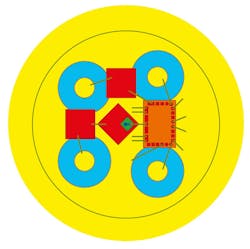
This is commonly achieved by using monolithic bare-die TIA ASICs that are located side-by-side in close proximity to the APD within a suitable optical sub-assembly package (Fig. 1).
The TIA output will be converted from a single-ended signal to a high-speed differential output using an SE-to-Diff stage followed by a differential output buffer driver. A steep roll-off filter is often incorporated into the signal chain to remove noise above the bandwidth of interest.
TIAs for optical communications are designed to meet industry-standard protocols and data rates. They don’t have as many degrees of freedom to consider compared to LRF and LiDAR in the TIA development phase.
Protocols are often designed to have DC-balanced data patterns that don’t upset DC-feedback loops in the signal path, unlike LRF and LiDAR whose data is much more burst-like and unbalanced. As the transmitted laser light is contained within an optical fiber cable, there’s no requirement to compensate for ambient sunlight.
>>Download the PDF of this article
However, overload and saturation are still potential problems when a high-powered transmitter is connected with a short fiber into a receiver without any bit errors for loopback testing purposes. Therefore, the TIA must operate over a large dynamic range, error-free, with a large bandwidth while achieving the best sensitivity. This represents the art of designing and interfacing TIAs for high-speed optical communications.
TIAs for Optical Time-Domain Reflectometry (OTDR)
While OTDR test equipment is mainly used to investigate and debug installed fiber in optical communications systems, the requirements for the TIAs are similar to those for LRFs, rather than those designed for high-speed communications. But the APD active area is smaller than that used in LRF and similar to that used in optical communications, since the transmitter and received light are coupled into a small-aperture glass fiber.
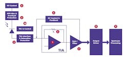
Design Considerations for TIA Applications (Fig. 2)
- The transimpedance-amplifier stage is the common key circuit element between all three applications considered. Implementation of the TIA circuit varies greatly though: LRF favors discrete components and op-amp ICs; LiDAR often uses dedicated op-amp ICs and ASICs; high-speed communications almost always uses bare die TIA ASICs due to the high-bandwidth requirements. For the lowest noise and best sensitivity, the gain should be maximized, but this can result in stability issues, especially at higher bandwidths and with large dynamic range changes. Selecting an APD that has the lowest noise and high intrinsic gain can help reduce the burden and compromises made in the TIA design and avoid stability issues.
- The feedback resistor determines the gain-bandwidth product of the TIA in conjunction with the photodiode capacitance and front-end parasitic capacitance of the TIA. Minimizing the input capacitance presented to the TIA can help reduce TIA noise. Therefore, selecting an APD with a low input capacitance relative to its active area can be helpful.
- APDs require high reverse bias voltages to operate in the avalanche region, typically upwards of 40 to 200 V. APD gain should be optimized for noise (especially in LRF and LiDAR applications) and bandwidth (especially in high-speed communications), which always presents a tradeoff for the designer. The high-voltage bias supply is often generated outside the optical sub-assembly packaging and fed in via an interface pin. To prevent APD (and TIA) overload conditions, a series resistor can be added on the bias side of the APD connection.
- Sophisticated high-voltage bias control circuits are often required and deployed to control the APD bias voltage across temperatures to maintain constant APD gain. Again, selecting an APD with a lower intrinsic noise can reduce the complexity of over-temperature bias controls.
- The interface between the APD and TIA is critical to performance; any parasitic capacitance and inductance should be reduced. External passive components or dump diodes can be utilized to reduce saturation of the TIA. In high-speed communications, this interface is typically just a single bondwire directly connected between the APD and TIA.
- DC correction and feedback loops are often used in TIA designs to reduce input offsets and improve sensitivity across the dynamic input range. However, these can lead to instability and longer recovery times. LRF applications are less likely to use DC cancellation loops, but these are used in LiDAR to compensate for ambient sunlight and in high-speed communications to improve the dynamic range.
- Typically proceeding the TIA are further voltage gain stage(s) and functions like single-ended to differential conversion and/or low-pass signal filtering.
- The output driver block presents a single-ended or differential signal in a controlled output impedance to interface with the proceeding signal processing.
- Signal processing is often an ADC for LRF, LiDAR, and OTDR, or a quantizer post-amplifier and retimer for high-speed communications.
- For some extremely low noise requirements in LRF and LiDAR, a thermoelectric cooler (TEC) is used within the optical package, which the APD is mounted upon, to accurately control the APD temperature relative to the ambient temperature and reduce the APD noise. These are bulky, expensive, and complex elements to design into the optical packaging, so using an APD with intrinsically low noise could avoid using a TEC to save cost and design effort. Finally, TECs are power-hungry—eliminating them will reduce system power requirements significantly.
Get to Know TIAs and APDs
TIAs are an essential circuit block for interfacing with infrared sensors, such as APDs. There are many application-dependent considerations for the designer during the development process. A good understanding of the characteristics of the APD being used, together with a “toolbox” of circuit implementation techniques, will help designers select the right components and optimize the performance of the intended application.
Designers should contact their APD supplier's application support team for best-practice advice, up-to-date information, and design guidance.
>>Download the PDF of this article
About the Author

Christian Rookes
CMO, Phlux Technology
Christian Rookes is CMO at Phlux Technology, a manufacturer of avalanche-photodiode (APD) infrared sensors based in Sheffield, UK. He has over 25 years’ experience in technical marketing in semiconductor and optical communication fields. Christian holds a BSc in Engineering and Physics from Loughborough University and an MBA Essentials Certificate from the London School of Economics. He holds two patents, including one related to impedance matching for laser diode circuits.


