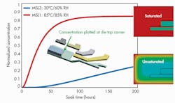
Have you ever wondered how to eliminate internal delamination inside your semiconductor package, or how to reduce warpage of your large ball-grid array (BGA) package to eliminate non-wets during board mounting? Semiconductor package modeling can help tackle some of these key challenges.
This file type includes high resolution graphics and schematics when applicable.
Related
New packaging solutions are continuously being developed to meet new performance and cost goals in a number of growing applications. Notable developments include solder flip-chip, copper pillar flip-chip, clip attachment to die, quad-flat no-lead (QFN), and wafer-level packages. One of the fundamental requirements of any packaging solution is mechanical integrity and reliability, which has also seen steady improvement through materials and process developments.
As the complexity increases, mechanical modeling tools and methodologies have also been developed to better design these new solutions. Simulation techniques have been developed to address several fail modes and performance metrics. Most of them address solder joint cracking, package internal delamination/cracking, and warpage at the package or strip level.
Warpage Modeling
Large-area array packages, or even small ball diameter and pitch packages, need to have well-controlled warpage resulting from temperature variation. Large warpage could lead to poor solder joint formation during surface mounting of packages onto printed-circuit boards (PCBs). Bad solder joints are typically non-wets or poorly shaped joints and lead to premature cracking during board-level temperature cycling.
In some cases, warpage is important even during package fabrication, such as during package singulation or while handling highly warped strips during assembly steps. Its primary cause is thermal expansion mismatch between different materials within the package. The coefficient of thermal expansion (CTE) of silicon die is much smaller than other materials in the package, like the organic substrate core, mold compound, die-attach material, and copper traces. Large mismatch leads to stress buildup, which is relieved partially by bending, resulting in a warped package.
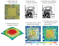
Figure 1 illustrates warpage modeling along with substrate traces for computational efficiency. Detailed trace geometry can be imported into mechanical simulation tools for warpage analysis through the finite element method (FEM). Detailed trace approach starts to become prohibitively expensive for large packages and substrates with many metal levels.
A simpler approach would be to approximate detailed trace geometry with an effective property representation of material boundaries using interpolation. This leads to much smaller and manageable models. For the example shown in Figure 1, the image-based effective property model took less than 15 minutes for the entire simulation, whereas the detailed model took more than an hour. It is not uncommon for an order of magnitude difference in simulation times for more complex devices.
With regard to accuracy, the simpler approach predicts warpage within 10% of the detailed model. In addition to warpage, copper-traces fatigue cracking during temperature cycling could lead to electrical opens. One simple metric to compare trace-cracking risk for different designs is the Von-Mises stress within the traces, also called equivalent stress. Figure 1e and 1f show remarkable prediction with simpler models in capturing global variation of the Von-Mises stress. This variation then can be used in a set of smaller sub-models localized to higher stress areas to analyze trace-cracking risk.
Particle-Based Material Modeling
Many of the organic-based materials in a semiconductor package are composites of filler particles embedded in a polymer matrix. Molding compounds and flip-chip underfill materials are typically filled with silica particles, although the volume fraction is quite different between the two classes of materials. Others, such as die attach and thermal interface material, are typically filled with silver flakes.
Variation of the volume fraction and size distribution of filler particles results in the simultaneous variation of a number of effective properties of the composites. This requires a good understanding of the functional dependence of effective properties with respect to filler particle distribution. Although analytical solutions are available, simulations with detailed particle representation can more precisely capture the variation of effective properties over a large range of distributions.
Techniques for particle-based material modeling have been developed and applied for several physical properties such as effective modulus, CTE, and thermal conductivity. These simulations include hundreds and thousands of particles in a representative volume element (RVE). The primary challenges of these techniques are obtaining an adequate distribution of particles and accurate meshing of the large number of particles.
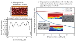
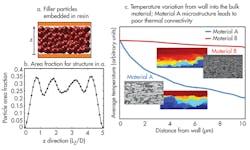
One interesting application is on the interaction of particle distribution with an interface resulting in reduced effective area fraction near the interface (Fig. 2a and 2b). Reduced area fraction leads to high thermal resistance near interfaces in series with bulk thermal resistance and can limit the effectiveness of a die-attach material. Using an image-based particle representation of two different die-attach materials (Fig. 2c), thermal simulations indicate a high temperature gradient near the interface resulting from particle sizes and distribution in Material B.
Delamination Risk Modeling
One of the leading mechanical fail modes in a semiconductor package is delamination between interfaces during reflow and temperature cycling. Delamination leads to higher thermal resistance if it is in a high heat flow path. It can also cause wire stitch break if it is on leads or a die paddle. Or, it can lead to ball bond breaks if the delamination is on the die top surface, leading to electrical opens. Predicting the delamination risk at an interface is complicated due to mechanical stress singularities near corners and edges, where the risk is typically highest for delamination initiation. Techniques based on advanced interface fracture mechanics are commonly employed to predict interface delamination.
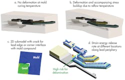
Fracture mechanics-based approaches typically involve a global analysis using conventional thermo-mechanical simulation and a local fracture sub-model to extract stress intensity factors or energy release rate near the crack tip. Figure 3 presents an example of lead delamination risk modeling for a small-outline integrated circuit (SOIC). Thermo-mechanical stresses due to CTE mismatch lead to stress buildup on lead edges and corners in this package during reflow temperature.
A number of 2D local crack models are simulated along the periphery of leads using displacements from the global model. These local sub-models provide the energy release rate, which is the energy available to open a unit area of crack. The larger this value, the greater the risk for delamination. Simulations reveal that the corner lead tip closer to the die has a relatively higher risk for delamination. Modifying the lead frame design could mitigate this risk.
Moisture Diffusion Modeling
Organic materials within a semiconductor package also absorb moisture from the air. Water molecules find their way through available free volume within the polymer network to reach critical internal interfaces. These water molecules generally lead to lower adhesion strength of the interface. Combined with high saturated pressure at reflow temperatures of 260°C, water expansion can cause delamination, with loud cracking sounds in some instances—also known as the popcorn effect. The concentration of moisture at interfaces determines the extent of delamination risk, which in turn depends on the diffusion properties of the polymer-based materials and package design.
Moisture concentration at interfaces can be predicted using diffusion modeling. A simple thermal-diffusion analogy can be used for constant temperature and fixed concentration boundary conditions. A direct concentration approach is needed for more complex time-varying fields. The influence of soak conditions needed for different moisture sensitivity level (MSL) requirements can be captured using the thermal-diffusion analogy.
Figure 4 shows the same SOIC package analyzed for delamination subjected to MSL1 and MSL3 soak conditions. In this case, mold properties and package dimensions result in a saturated condition for MSL1 and a far from saturated condition for MSL3. Such simulations coupled with delamination modeling help to confirm new designs are within the qualified design space with respect to MSL reliability.
What’s Next?
There have been exciting developments of new techniques for the mechanical integrity and reliability assessment of semiconductor packages. These include warpage, moisture diffusion, delamination, and material modeling. Although 3D simulations of many of the complex devices are within reach, further developments are needed to fully integrate them into the design flow while still keeping short cycle times.
Key challenges include fully automated meshing, mesh-independent post-processing, accurate measurement of nonlinear material characteristics, and low computational cost. Overcoming these challenges will bring us much closer to enabling the mechanical assessment of every device before assembly and qualification.
Siva P. Gurrum is a member of the Group Technical Staff at Texas Instruments. He received his BTech degree in 1999 from the Indian Institute of Technology, Madras, his MS in 2001 from the University of Maryland at College Park, and his PhD in 2006 from Georgia Institute of Technology, all in mechanical engineering. At TI, he has worked on thermal and thermo-mechanical analysis for semiconductor packages including modeling and characterization. He also has authored and coauthored more than 20 papers, has written one book chapter, and holds five U.S. patents. He can be reached at [email protected].
Comments
Comments
