The P7 was the first prototype for an op amp to use a varactor diode bridge as a means of producing an error signal amplified by transistors (rather than the conventional vacuum tubes or, later on, FETs). Conceptualized by George A. Philbrick (or Lewis R. Smith?), the prototype was simplified (well, a nitpicker may argue the extra circuit current) by Bob Malter, resulting in one of the most profitable operational amplifiers ever to be sold—the P2.
Sporting input bias currents in the picoampere range (1x10-12), the P2 cost $220, which was 1/8 to 1/2 (my source for this one is obscure) the price of a VW Beetle at the time. The cost of building a P2 paralleled that of a cheap radio—around $10 to $15—so you can just imagine how lucrative things were in those days. The P2 dominated for 30 years, becoming obsolete only after the release of the LMC660, which now offers input bias currents at the femtoampere range (1x10-15).
My interest for the P2 was piqued once more by Paul Rako’s great post “What’s All this Varactor Input Amplifier Stuff, Anyhow?” In the article, he delved into an improved schematic from the late Bob Pease and attempted a computer simulation out of it, an endeavor that proved partially unsuccessful due to unaccounted parasitics and magnetics. (I can hear Mr. Pease’s voice from the heavens right now shouting “What are you guys doing with my circuit on a computer?!”)
Anyway, we found out from the comments that LTSpice had the older form of the circuit, the P2, as an educational example. I am embarrassed myself of not knowing it was there, and fortunate to discover that it was. So, here was a circuit, a high-profile industrial secret 40 years ago, free to the public for tweaking and vandalizing. It’s an opportunity to expand our horizons on op-amp function and design, so I had a go at a couple of simulations, discussed below. Hopefully, I don’t hear Mr. Philbrick’s voice shouting at me anytime soon.
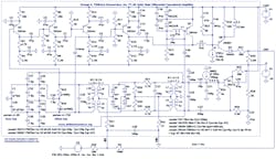
1. Schematic of the P2 in LTSpice. (Click image to enlarge)
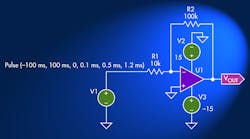
The op amp is configured as a simple inverting amplifier. The source is a pulse generator at 200 mV p-p [0 V dc offset] with an on and off time of 0.5 ms. Rise and fall times are set to 0.1 ms. (Why? Bob Pease mentioned in Jim William’s book that the slew rate of the P2 was awful – 0.03V/µsec. The P2 needed 33.33 µs to reach 1V at the output. Yuck! We’ll see the tolerance range for the rise and fall times in Part 2, where the circuit is truly vandalized.) All current is flowing at R35 and the feedback resistor R3; 10 µA will induce a 1-V drop at R3. Since the other terminal is referenced to ground, the output voltage during the positive cycle of the input will be an inverted 1 V (and vice versa during the negative cycle).
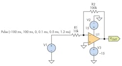
The alternative textbook formula (which I’ve grown to hate) for the gain of an inverting op amp is –Rf/Ri. Such shortcuts have become lethargic to me. Solving yields –(100 kâ¦/10 kâ¦) = –10.
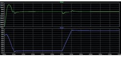
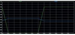
You yourself may try the simulation out, and due to excitement, get an immediate figure similar to the one shown here:
2. Immediate simulation result of the P2 in LTSpice. (Click image to enlarge)
The input is, of course, at the end of the resistor pulled down to ground by the coils of the bridge. You won’t get that from an ideal op amp (redrawn below for convenience):
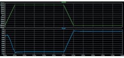
For comparison, below is the simulation result of the P2 with the probe on the input pulse.
The strange trend at the output between 0 ms to 0.1 ms is because the output hasn’t yet reached 1 V. Therefore, I introduced a delay of 0.1 ms to ensure that the cause isn’t effectuated by the startup of the circuit.
6. Simulation result of the P2 with a delayed pulse. (Click image to enlarge)
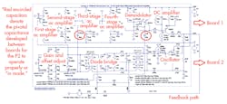
The next step is to figure out the functions of each branch in the circuit. If my assumptions are correct, the labeled figure below should suffice to properly identify each region:
The oscillator feeds a sinusoidal “carrier” to the diode bridge to modulate the inputs. The transformers provide dc isolation. In reality, two pairs of well-matched diodes offset the leakage currents to a minimum:
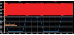
The simulation result for the output of the balanced bridge and gain/offset adjust is illustrated below:
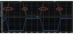
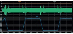
Four stages of ac amplification later yields this waveform:
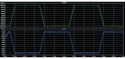
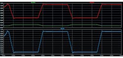
After demodulation and dc amplification, the dc offset is brought down by the resistor-divider network at the output:
11. Output of dc amplifier. (Click image to enlarge)
So, this is how the P2 amplifier works. Apparently, I tried to remove the capacitor that represented the stray capacitances of the circuit (did it include the Miller capacitance?), but had no observable effect.
Then, I tried removing C40 and poof! The output railed to the negative supply! Was this the same phenomenon that Burr-Brown’s rumored infamous, ill-fated engineer experienced on his testbench those many decades ago?
If you have downloaded LTSpice, why not give it a try and share your thoughts or ideas on the matter.
